Copyright © Siemens AG 2016. All rights reserved
474
ERTEC 200P-2 Manual
Technical data subject to change
Version
1.0
4 LAYOUT AND DESIGN HINTS
4.1 EMC Measures
4.1.1 ESD Protection
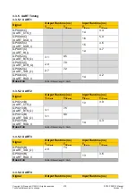
With the 3.3 V input cells, there is a sufficient clearance from the ESD structure triggering.
o
ESD characteristics CB55, 3.3 V I/O buffer:
Trigger voltage (Vt1): ca. 9 V
Hold voltage (Vhold): ca. 5 V
VDDmax:
3.6 V (3.3 V + 10%)
With the 1.8 V input cells, there is a sufficient clearance from the ESD structure triggering.
o
ESD characteristics CB55, 1.8 V I/O buffer:
Trigger voltage (Vt1): ca. 7 V
Hold voltage (Vhold): ca. 4 V
VDDmax:
1.9 5V (1.8 V + 10%)
4.1.2 Immunity to ESD
HBM: 1000 V
SDM/CDM: 500 V
4.1.3 Package Power Distribution
There was a focus on "good distribution" of the supply pins in the ballout.
short discharge paths between protective structure and supply ball are guaran-
teed
Optimization of the I/O ring and the package PCB ensures better signal integrity and im-
proves the discharge capacity of the supply pins
Leakage current and signal [return] current respond in a similar way.
4.1.4 Spike Filter
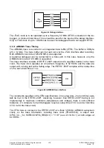
The same spike filters are implemented for the test inputs TAP_SEL and TACT at the input
as for the reset inputs (XRESET, XSRST, XTRST). The filters ensure that spikes <= 40 ns
(best case) are suppressed. This ensures a time constant of 40 ns between the pin and
function (low-pass).
Note: A spike at TAP_SEL and/or TACT is not usually forwarded to the JTAG controller as
this would require a sequence over TDI/TMS and TCK from the debugger.
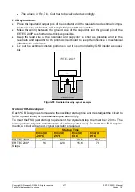
The ERTEC 200P does contain a spike filter of 40 ns (best case condition) for following
signals:
XRESET (Power-On Reset)
XSRST (Debugger-Reset)
XTRST (JTAG Reset)
TAP_SEL (TAP Select)
TACT (Testmode)


