Copyright © Siemens AG 2016. All rights reserved
12
ERTEC 200P-2 Manual
Technical data subject to change
Version
1.0
List of Figures
Figure 1: ERTEC 200P use cases
Figure 2: Application operation with external host
Figure 3: Application operation without external host
Figure 4: ERTEC 200P Step2 block diagram
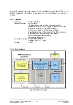
Figure 5: ARM926 subsystem
Figure 6: JTAG chain
Figure 7: AHB/APB bridge, block diagram
Figure 8: APB bridge, timing
Figure 9: EMC Block Diagram
Figure 10: EMC interface with two SDRAM / two Burst Flash configuration
Figure 11: EMC interface with only one SDRAM / one Burst Flash configuration
Figure 12: EMC interface with asynchronous RAM
Figure 13: EMC, Address Space
Figure 14: EMC, Notation definition for a read access (ASYNC)
Figure 15: EMC, Notation definition for a write access (ASYNC)
Figure 16: EMC, Application Example SDRAM
Figure 17: EMC, Application example: Combination of SDRAM and asynchronous
Interfaces
Figure 18: EMC, Interface Signals
Figure 19: Block diagram of the host interface
Figure 20: XHIF, Symbol and Signals
Figure 21: XHIF interface adjustment
Figure 22: Block diagram of the peripheral interface
Figure 23: Block diagram of PN-ICU for PN_IRQx(0/1:0) group interrupts
Figure 24: Block diagram of PN-MUX for PN_IRQx(2:1/15:2) single interrupts
Figure 25: PNPLL with 3 application time blocks (application connection)
Figure 26: Quartz wiring
Figure 27: Clock source for the Ethernet connection
Figure 28: ERTEC 200P reset matrix
Figure 29: PLL startup phase
Figure 30: Block diagram of the IO filter
Figure 31: Block diagram of the filter structure of a channel
Figure 32: Block diagram of the central clock divider
Figure 33: Signal in signal filtering
Figure 34: Block diagram ARM926 Watchdog
Figure 35: XWD_OUT0/ WD_INT signal sequence
Figure 36: XWD_OUT1 signal sequence
Figure 37:TIMER block diagram
Figure 38: F-timer block diagram
Figure 39: Baud rates UART when F
UARTCLK
= 125 MHz
Figure 40: SPI Block Diagram
Figure 41: SPI flash: serial output timing
Figure 42: SPI flash: serial input timing
Figure 43: Block diagram of a GPIO module
Figure 44: GPIO, IO Circuit


