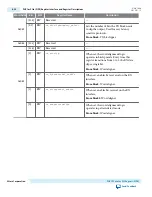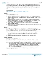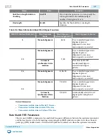
Name
Value
Description
Base data rate
1 × Data rate
2 × Data rate
4 × Data rate
The base data rate is the frequency of the clock input
to the PLL. Select a base data rate that minimizes the
number of PLLs required to generate all the clocks
required for data transmission. By selecting an
appropriate base data rate, you can change data rates
by changing the divider used by the clock generation
block. For higher frequency data rates 2 × and 4×
base data rates are not available.
Input clock frequency
Variable
Specifies the frequency of the PLL input reference
clock.
Additional Options
Enable TX Bitslip
On/Off
When enabled, the TX bitslip word aligner is
operational.
Create rx_coreclkin port
On/Off
This is an optional clock to drive the coreclk of the
RX PCS
Create tx_coreclkin port
On/Off
This is an optional clock to drive the coreclk of the
TX PCS
Create rx_recovered_clk
port
On/Off
When enabled, the RX recovered clock is an output.
Create optional ports
On/Off
When you turn this option on, the following signals
are added to the top level of your transceiver for each
lane:
•
tx_forceelecidle
•
rx_is_lockedtoref
•
rx_is_lockedtodata
•
rx_signaldetect
Enable Avalon data
interfaces and bit reversal
On/Off
When you turn this option On, the order of symbols
is changed. This option is typically required if you
are planning to import your Custom PHY IP Core
into a Qsys system.
9-6
General Options Parameters
UG-01080
2015.01.19
Altera Corporation
Custom PHY IP Core
Send Feedback


