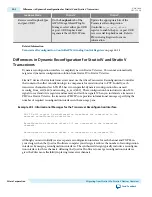
Stratix IV GX Device Signal Name
(21)
Stratix V GX Device Signal Name
Width
Not available
phy_mgmt_clk_reset
1
phy_mgmt_clk
1
phy_mgmt_address
[8:0]
phy_mgmt_read
1
phy_mgmt_readdata
[31:0]
phy_mgmt_write
1
phy_mgmt_writedata
[31:0]
Related Information
PHY for PCIe (PIPE) Register Interface and Register Descriptions
on page 8-15
Differences Between Custom PHY Parameters for Stratix IV and Stratix V
Devices
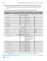
This section lists the Custom PHY parameters and the corresponding ALTGX megafunction parameters.
Table 20-6: Comparison of ALTGX Megafunction and Custom PHY Parameters
ALTGX Parameter Name (Default Value)
Custom PHY Parameter Name
General
Not available
Device family
Transceiver protocol
Mode of operation
Enable bonding
What is the number of channels?
Number of lanes
Which subprotocol will you be using? (×4, ×8) Not available
What is the channel width?
Serialization factor
What is the effective data rate?
Data rate
What is the input clock frequency?
Input clock frequency
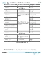
tx/rx_8b_10b_mode
Enable 8B/10B encoder/decoder
Not available
Enable manual disparity control
Create optional 8B10B status ports
(21)
<
n
> = the number of lanes. <
d
> = the total deserialization factor from the pin to the FPGA fabric.
UG-01080
2013.12.20
Differences Between Custom PHY Parameters for Stratix IV and Stratix V Devices
20-11
Migrating from Stratix IV to Stratix V Devices Overview
Altera Corporation
Send Feedback


