

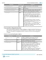


Reconfig Addr
Bits
R/W
Register Name
Description
7’h1A
[9]
R
control and status
Error
.When asserted, indicates an invalid
channel or address.
[8]
R
Busy
. When asserted, indicates that a
reconfiguration operation is in progress.
[1]
W
Read
. Writing a 1 to this bit triggers a read
operation.
[0]
W
Write
. Writing a 1 to this bit triggers a
write operation.
7’h1B
[5:0] RW
dfe_offset
Specifies the 6-bit offset of the DFE
register.
7’h1C
[15:0] RW
data
Reconfiguration data for the transceiver
PHY registers.
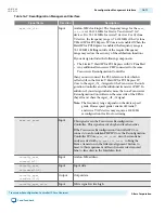
The following table describes the DFE registers that you can access to change DFE settings.
Note: All undefined register bits are reserved.
Table 16-14: DFE Offset and Values
Offset
Bits
R/W
Register Name
Description
0x0
[1]
RW
power on
Writing a 0 to this bit powers down DFE in the
channel specified.
[0]
RW
adaptation engine enable
Writing a 1 enables the adaptive equalization
engine.
0x1
[3:0] RW
tap 1
Specifies the coefficient for the first post tap. The
valid range is 0–15.
0x2
[3]
RW
tap 2 polarity
Specifies the polarity of the second post tap as
follows:
• 0: negative polarity
• 1: positive polarity
[2:0] RW
tap 2
Specifies the coefficient for the second post tap.
The valid range is 0–7.
0x3
[3]
RW
tap 3 polarity
Specifies the polarity of the third post tap as
follows:
• 0: negative polarity
• 1: positive polarity
[2:0] RW
tap 3
Specifies the coefficient for the third post tap.
The valid range is 0–7.
UG-01080
2015.01.19
Transceiver Reconfiguration Controller DFE Registers
16-21
Transceiver Reconfiguration Controller IP Core Overview
Altera Corporation
Send Feedback