


30 Hardware description
Manual Energy Storage Inverter ESI-S
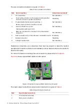
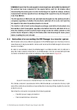
Table 13: ESI main controller board description
Item Description
Circuit diagram
designation
1
System connector: 24 V power supply to control board
P2
2
CAN bus connection from previous inverter unit
P20
3
CAN bus connection to next inverter unit
P21
4
System connector: Power supply and CAN communication to ESI-
Manager
P4
5
System connector: 230 V power supply to control board
P3
6
System connector: Spare
P19
7
System connector: Main contactor control
P18
8
System connector: Spare
P17
9
System connector: Fan control
P16
10
System connector: Monitoring temperature of PWM and Line
reactors
P25
11
System
connector:
Spare
P7
12
System connector: Coming from CT terminal X21 (internal)
P5
13
System connector: Supply and DC link voltage measurement
P6
14-15-16 System connectors: Spare
P9, P10, P11
17
System
connector:
control
of
IGBT-module
P12
18
Voltage selector DIP-switch : Not used in ESI-S (single voltage)
19
System
LED’s
(top
to
bottom)
LED 3: ON: Critical error in inverter unit considered (red LED)
LED 3: OFF: No critical error in inverter unit considered
LED 2: ON: ESI unit running or in startup process (Armed)
LED 2: OFF: ESI unit off and not in startup process
LED 1: Blinking at regular interval (1 s): Microcontroller running
properly
LED 1: ON, OFF or blinking irregularly: Microcontroller not running
properly
20
System
LED’s
(top
to
bottom)
LED 5: ON: Inverter unit is acting as the master of the complete
system
LED 5: OFF: Inverter unit is acting as a slave in the inverter system
LED 4: Blinking at regular interval (1 s): DSP processor running
properly
LED 4: ON, OFF or blinking irregularly: DSP processor not running
properly
21
PQF-Link communication opto-isolated
serial link connector
22
Inverter unit address selector (3 Left most DIP switches) and CAN
bus termination (Right hand DIP switch):
Symbols used: L: low – H: high