


GD32E23x User Manual
508
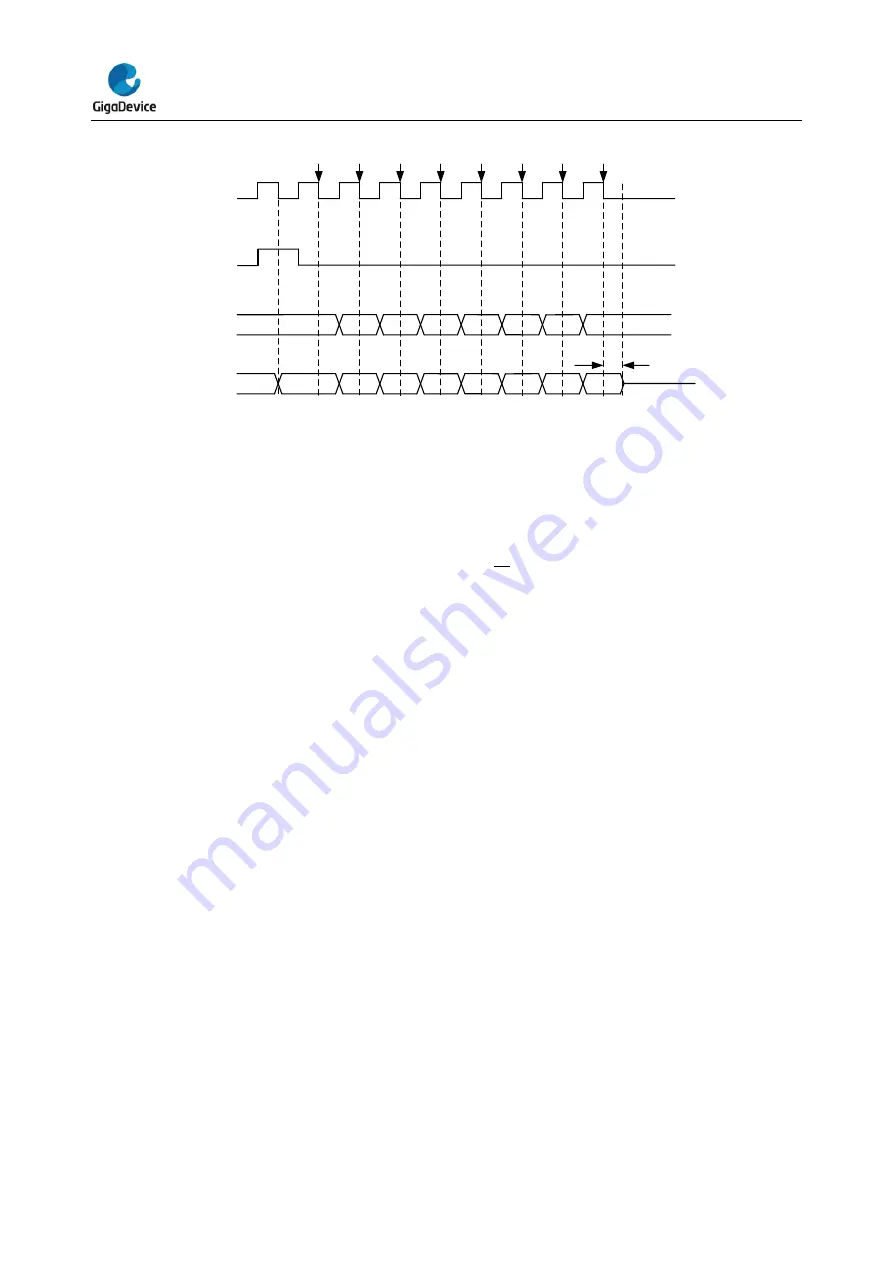
Figure 18-13. Timing diagram of TI slave mode
D[7]
D[6]
D[5]
D[4]
D[3]
D[2]
D[1]
D[0]
D[7]
D[6]
D[5]
D[4]
D[3]
D[2]
D[1]
D[0]
SCK
NSS
MOSI
MISO
sample
Td
In slave TI mode, after the last rising edge of SCK in transfer, the slave begins to transmit the
LSB bit of the last data byte, and after a half-bit time, the master begins to sample the line.
To make sure that the master samples the right value, the slave should continue to drive this
bit after the falling sample edge of SCK for a period of time before releasing the pin. This
time is called
T
d
,
T
d
is decided by PSC [2:0] bits in SPI_CTL0 register.
T
d
=
T
bit
2
+5*T
pclk
(17-1)
For example, if PSC [2:0] = 010,
T
d
is 9*T
pclk
.
In slave mode, the slave also monitors the NSS signal and sets an error flag FERR if it
detects an incorrect NSS behavior, for example: toggles at the middle bit of a byte.
NSS pulse mode operation sequence
This function is controlled by NSSP bit in SPI_CTL1 register. In order to implement this
function, several additional conditions must be met: configure the device to master mode,
frame format should follow the normal SPI protocol, select the first clock transition as the
data capture edge.
In summary, MSTMOD = 1, NSSP = 1, CKPH = 0.
When NSS pulse mode is enabled, a pulse duration of at least 1 SCK clock period is inserted
between two successive data frames depending on the status of internal data transmission
buffer/TXFIFO. Multiple SCK clock cycle intervals are possible if the transfer buffer/TXFIFO
stays empty. This function is designed for single master-slave configuration for the slave to
latch data. The following diagram depicts its timing diagram.


