


GD32E23x User Manual
424
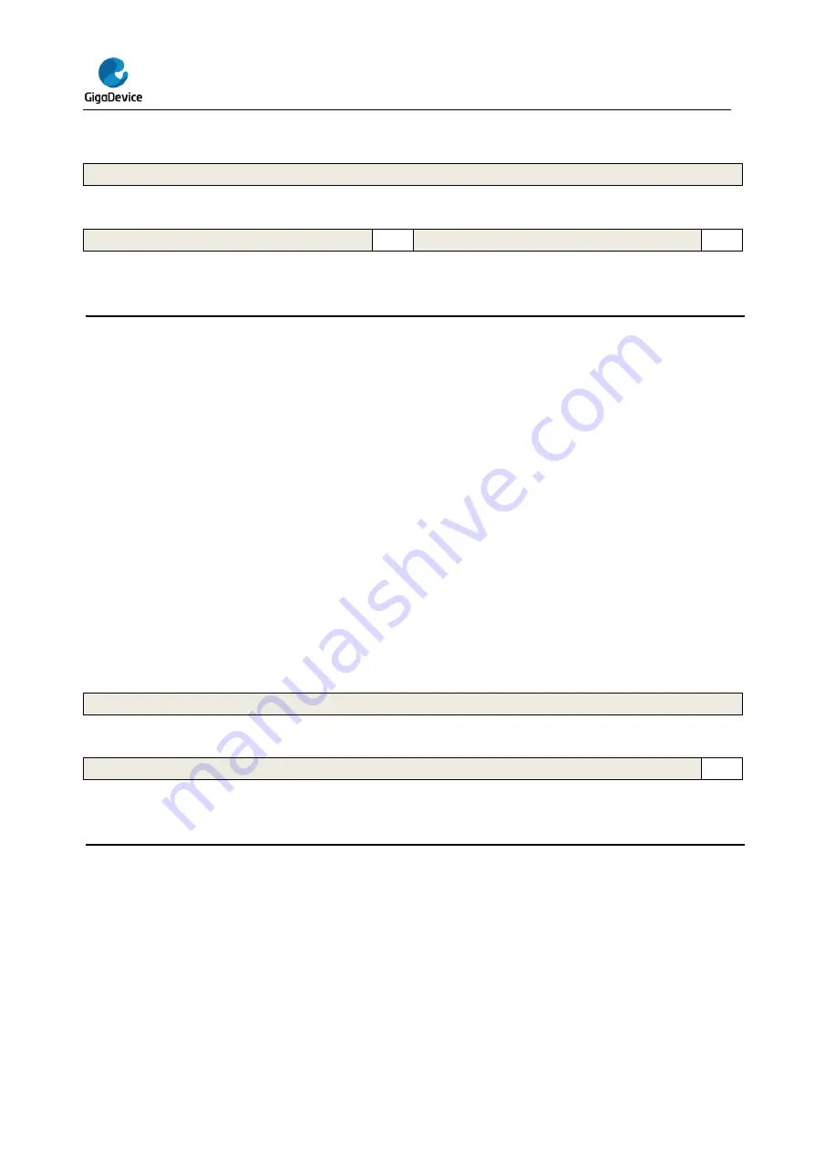
This register has to be accessed by word(32-bit)
31
30
29
28
27
26
25
24
23
22
21
20
19
18
17
16
Reserved
15
14
13
12
11
10
9
8
7
6
5
4
3
2
1
0
Reserved
UPDEN
Reserved
UPIE
rw
rw
Bits
Fields
Descriptions
31:9
Reserved
Must be kept at reset value.
8
UPDEN
Update DMA request enable
0: disabled
1: enabled
7:1
Reserved
Must be kept at reset value.
0
UPIE
Update interrupt enable
0: disabled
1: enabled
Interrupt flag register (TIMERx_INTF)
Address offset: 0x10
Reset value: 0x0000 0000
This register has to be accessed by word(32-bit)
31
30
29
28
27
26
25
24
23
22
21
20
19
18
17
16
Reserved
15
14
13
12
11
10
9
8
7
6
5
4
3
2
1
0
Reserved
UPIF
rc_w0
Bits
Fields
Descriptions
31:1
Reserved
Must be kept at reset value.
0
UPIF
Update interrupt flag
This bit is set by hardware on an update event and cleared by software.
0: No update interrupt occurred
1: Update interrupt occurred
Software event generation register (TIMERx_SWEVG)
Address offset: 0x14


