MB95630H Series
MN702-00009-1v0-E
FUJITSU SEMICONDUCTOR LIMITED
429
CHAPTER 21 MULTI-PULSE GENERATOR
21.6 Registers
21.6.2
16-bit MPG Output Control Register (Lower)
(OPCLR)
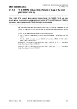
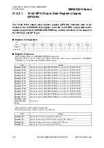
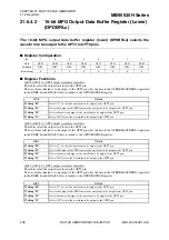
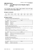
The 16-bit MPG output control register (lower) (OPCLR) controls the output of
the OPT5 to OPT0 pins and the position detection interrupt.
■
Register Configuration
■
Register Functions
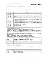
[bit7] PDIF: Position detection interrupt request flag bit
This bit is the position detection interrupt request flag.
This bit is set to "1" when either one of the following conditions occurs:
• The CMPE bit in the IPCUR register is set to "1" and the SNI2 to SNI0 pins are compared with the RDA[2:0]
bits and they match.
• The CMPE bit is set to "0" and an effective edge is detected at SNI2 to SNI0 pins.
With the position detection interrupt already enabled (PDIE = 1), when the PDIF bit is set to "1", a position
detection interrupt is generated.
Writing "0" to this bit clears it. Writing "1" to this bit has no effect on operation.
When read by the read-modify-write (RMW) type of instruction, this bit always returns "1".
[bit6] PDIE: Position detection interrupt enable bit
This bit enables or disables the position detection interrupt.
When this bit is set to "1", and the position detection interrupt request flag bit (PDIF) is also set to "1", a
position detection interrupt is generated.
[bit5] OPE5: OPT5 output enable bit
This bit enables or disables OPT5 pin output.
bit
7
6
5
4
3
2
1
0
Field
PDIF
PDIE
OPE5
OPE4
OPE3
OPE2
OPE1
OPE0
Attribute
R/W
R/W
R/W
R/W
R/W
R/W
R/W
R/W
Initial value
0
0
0
0
0
0
0
0
bit7
Details
Reading "0"
Indicates that no position detection interrupt request has been generated.
Reading "1"
Indicates that a position detection interrupt request has been generated.
Writing "0"
Clears this bit.
Writing "1"
Has no effect on operation.
bit6
Details
Writing "0"
Disables the position detection interrupt.
Writing "1"
Enables the position detection interrupt.
bit5
Details
Writing "0"
Disables OPT5 pin output.
Writing "1"
Enables OPT5 pin output.


