MB95630H Series
254
FUJITSU SEMICONDUCTOR LIMITED
MN702-00009-1v0-E
CHAPTER 14 LIN-UART
14.7 Registers
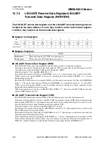
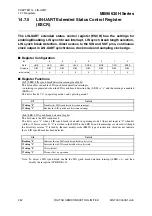
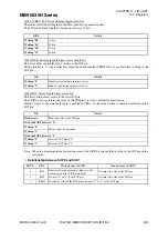
[bit1] CCO: Continuous clock output enable bit
This bit enables or disables continuous serial clock output from the SCK pin.
In operating mode 2 (synchronous) in which the serial clock transmission side is selected, setting the CCO bit
to "1" enables the continuous serial clock output from the SCK pin when the SCK pin is used as an clock
output pin.
Note: When the CCO bit is "1", set the SSM bit in the ECCR register to "1".
[bit0] SCES: Sampling clock edge select bit
This bit selects a sampling edge. In operating mode 2 (synchronous) in which the serial clock reception side
is selected, setting the SCES bit to "1" switches the sampling edge from the rising edge to the falling edge.
In operating mode 2 (synchronous) in which the serial clock transmission side is selected (ECCR:MS = 0),
when the SCK pin is used as an clock output pin, the internal serial clock signal and the output clock signal
are inverted.
In operating mode 0/1/3, set this bit to "0".
With this bit set to "1", executing a software reset is prohibited.
Disable reception and transmission before modifying this bit.
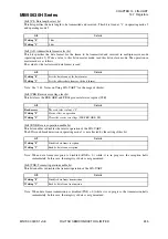
bit1
Details
Writing "0"
Disables continuous clock output.
Writing "1"
Enables continuous clock output.
bit0
Details (only for operating mode 2)
Writing "0"
Selects the rising edge of the clock as the sampling edge (normal).
Writing "1"
Selects the falling edge of the clock as the sampling edge (inverted clock).


