MB95630H Series
MN702-00009-1v0-E
FUJITSU SEMICONDUCTOR LIMITED
245
CHAPTER 14 LIN-UART
14.7 Registers
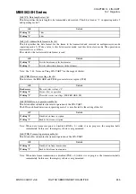
[bit4] CL: Data length select bit
This bit specifies the data length to be transmitted and received. This bit is fixed at "1" in operating mode 2
and operating mode 3.
[bit3] AD: Address/data format select bit
This bit specifies the data format for the frame to be transmitted and received in multiprocessor mode
(operating mode 1). Write a value to this bit in master mode; read this bit in slave mode. The operation in
master mode is as follows.
The value for the last received data format is read.
Note: See "14.8 Notes on Using LIN-UART" for the usage of this bit.
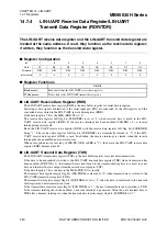
[bit2] CRE: Receive error flag clear bit
This bit clears the FRE, ORE, and PE flags in serial status register (SSR).
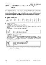
[bit1] RXE: Receive operation enable bit
This bits enables or disables the receive operation of the LIN-UART.
The LIN synch break detection in operating mode 3 is not affected by the setting of this bit.
Note: When data frame reception is disabled (RXE = 0) while it is in progress, the reception halts
immediately. In this case, the integrity of data is not guaranteed.
[bit0] TXE: Transmit operation enable bit
This bits enables or disables the transmit operation of the LIN-UART.
Note: When data frame transmission is disabled (TXE = 0) while it is in progress, the transmission halts
immediately. In this case, the integrity of data is not guaranteed.
bit4
Details
Writing "0"
7 bits
Writing "1"
8 bits
bit3
Details
Writing "0"
Sets the data frame as the data format.
Writing "1"
Sets the address data frame as the data format.
bit2
Details
Read access
The read value is always "0".
Writing "0"
Has no effect on operation.
Writing "1"
Clears the receive error flags (SSR:FRE, ORE, PE).
bit1
Details
Writing "0"
Disables data frame reception.
Writing "1"
Enables data frame reception.
bit0
Details
Writing "0"
Disables data frame transmission.
Writing "1"
Enables data frame transmission.

