MB95630H Series
MN702-00009-1v0-E
FUJITSU SEMICONDUCTOR LIMITED
457
CHAPTER 22 UART/SIO
22.2 Configuration
22.2
Configuration
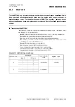
The UART/SIO consists of the following blocks:
• UART/SIO serial mode control register 1 (SMC1n)
• UART/SIO serial mode control register 2 (SMC2n)
• UART/SIO serial status and data register (SSRn)
• UART/SIO serial input data register (RDRn)
• UART/SIO serial output data register (TDRn)
The number of pins and that of channels of the UART/SIO vary among products. For details,
refer to the device data sheet.
In this chapter, "n" in a pin name and a register abbreviation represents the channel number.
For details of pin names, register names and register abbreviations of a product, refer to the
device data sheet.
■
Block Diagram of UART/SIO
Figure 22.2-1 Block Diagram of UART/SIO
Dedic
a
ted
bau
d r
a
te gener
a
tor
1/4
Pin
Pin
Pin
Clock
s
elector
Extern
a
l clock inp
u
t
UCKn
S
eri
a
l d
a
t
a
inp
u
t
UIn
S
t
a
rt
b
it
detection
Recep-
tion
b
it
co
u
nt
P
a
rity
oper
a
tion
S
hift
regi
s
ter
for
reception
UART/
S
IO
s
eri
a
l
inp
u
t d
a
t
a
regi
s
ter
UART/
S
IO
s
eri
a
l
s
t
a
t
us
a
nd
d
a
t
a
regi
s
ter
UART/
S
IO
s
eri
a
l
mode
control
regi
s
ter
s
1, 2
UART/
S
IO
s
eri
a
l
o
u
tp
u
t d
a
t
a
regi
s
ter
S
hift
regi
s
ter
for tr
a
n
s
-
mi
ss
ion
Tr
a
n
s
mi
s
-
s
ion
b
it
co
u
nt
P
a
rity
oper
a
tion
S
eri
a
l d
a
t
a
o
u
tp
u
t
UOn
S
eri
a
l clock o
u
tp
u
t
Port control
S
et to
e
a
ch
b
lock
Inter
n
a
l
bu
s
Reception
s
t
a
te
deci
s
ion
circ
u
it
PER
OVE
FER
RDRF
Tr
a
n
s
mi
s
-
s
ion
s
t
a
te
deci
s
ion
circ
u
it
TDRE
RIE
TEIE
Reception
interr
u
pt
Tr
a
n
s
mi
ss
ion
interr
u
pt
S
t
a
te from
e
a
ch
b
lock
S
t
a
te from
e
a
ch
b
lock
TCPL
TCIE
D
a
t
a
sa
mple clock inp
u
t


