MB95630H Series
MN702-00009-1v0-E
FUJITSU SEMICONDUCTOR LIMITED
283
CHAPTER 16 LOW-VOLTAGE DETECTION RESET CIRCUIT
16.2 Configuration
16.2
Configuration
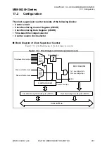
Figure 16.2-1 is the block diagram of the low-voltage detection reset circuit.
■
Block Diagram of Low-voltage Detection Reset Circuit
Figure 16.2-1 Block Diagram of Low-voltage Detection Reset Circuit
Re
s
et
s
ign
a
l
Vref
V
CC
N-ch
LVD re
s
et volt
a
ge
s
election ID regi
s
ter (LVDR)
LVR
S
7 LVR
S
6
LVR
S
4 LVR
S3
LVR
S
2 LVR
S
1 LVR
S
0
LVR
S
5
0xAA
0x5A
0x55
Other
v
a
l
u
e
s

