MB95630H Series
MN702-00009-1v0-E
FUJITSU SEMICONDUCTOR LIMITED
33
CHAPTER 3 CLOCK CONTROLLER
3.3 Registers
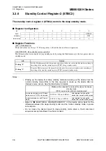
[bit4] SRST: Software reset bit
This bit sets the software reset.
The read value of this bit is always "0".
[bit3] TMD: Watch bit
This bit sets transition to time-base timer mode or watch mode.
Writing "1" to this bit in main clock mode, main CR clock, or main CR PLL clock mode causes the device to
transit to time-base timer mode.
Writing "1" to this bit in subclock mode or sub-CR clock mode causes the device to transit to watch mode.
Writing "0" to this bit has no effect on operation.
The read value of this bit is always "0".
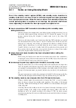
Note: After an interrupt request is generated, writing "1" to this bit is ignored. For details, see "3.5.1 Notes
[bit2:0] Undefined bits
Their read values are always "0". Writing values to these bits has no effect on operation.
Notes:
•
Set a standby mode after making sure that the transition to clock mode has been
completed by comparing the values of the clock mode monitor bits (SYCC:SCM[2:0])
and clock mode select bits (SYCC:SCS[2:0]) in the system clock control register.
•
If two or more of the following bits, stop bit (STP), sleep bit (SLP), software reset bit
(SRST) and watch bit (TMD), are set to "1" together, the order of priority for such bits
is as follows:
(1) Software reset bit (SRST)
(2) Stop bit (STP)
(3) Watch bit (TMD)
(4) Sleep bit (SLP)
When released from standby mode, the device returns to the normal operating state.
bit4
Details
Writing "0"
Has no effect on operation.
Writing "1"
Generates a 3-machine clock reset signal.
bit3
Details
In main clock mode, main CR clock mode
or main CR PLL clock mode
In subclock mode or sub-CR clock mode
Writing "0"
Has no effect on operation.
Has no effect on operation.
Writing "1"
Causes the device to transit to time-base timer
mode.
Causes the device to transit to watch mode


