MB95630H Series
410
FUJITSU SEMICONDUCTOR LIMITED
MN702-00009-1v0-E
CHAPTER 21 MULTI-PULSE GENERATOR
21.5 Operations
The comparison for the position detection is done in pair for each SNIx pin and RDAx bit
(SNI2 and RDA2, SNI1 and RDA1, SNI0 and RDA0), a comparison match starts the 16-bit
reload timer. The write signal is generated by the16-bit reload timer underflow.
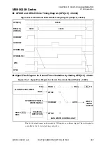
Pin OPTx output waveform according to the effective edge input to pin SNIx is shown in
Figure 21.5-19. The 16-bit reload timer is started when the pins SNI2 to SNI0 are compared
with the value of the RDA[2:0] bits and matches. Data transfer from the 16-bit MPG output
data buffer register (upper/lower) (OPDBRHx/OPDBRLx) specified by the RDA[2:0] bits to
the 16-bit MPG output data register (upper/lower) (OPDUR/OPDLR) is triggered by the
underflow of the 16-bit reload timer. The operation of output data is renewed automatically.
In order to use this method, the 16-bit reload timer should be used in one-shot mode. TIN0O
must be longer than two machine cycles.


