MB95630H Series
MN702-00009-1v0-E
FUJITSU SEMICONDUCTOR LIMITED
277
CHAPTER 15 8/10-BIT A/D CONVERTER
15.6 Registers
15.6.3
8/10-bit A/D Converter Data Register
(Upper/Lower) (ADDH/ADDL)
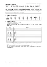
The 8/10-bit A/D converter data register (upper/lower) (ADDH/ADDL) store the
results of 10-bit A/D conversion during 10-bit A/D conversion.
The upper two bits of 10-bit data are stored in the ADDH register and the lower
eight bits the ADDL register.
■
Register Configuration
■
Register Functions
The upper two bits of 10-bit A/D data correspond to bit1 and bit0 in the ADDH register and the
lower eight bits bit7 to bit0 in the ADDL register.
If the AD8 bit in ADC2 register is set to "1", 8-bit precision is selected. Reading the ADDL
register can obtain 8-bit data.
These two registers are read-only registers. Writing data to them has no effect on operation.
In A/D conversion in which 8-bit precision is selected, SAR8 and SAR9 in the ADDH register
become "0".
●
A/D conversion function
When A/D conversion is started, the results of conversion are finalized and stored in the
ADDH and ADDL registers after the conversion time according to the register settings elapses.
After A/D conversion is completed and before the next A/D conversion is completed, read A/D
data registers (conversion results), and clear the interrupt request flag bit (ADI) in the ADC1
register. During A/D conversion, the values of the ADDH and ADDL registers are results of
the last A/D conversion.
ADDH
bit
7
6
5
4
3
2
1
0
Field
—
—
—
—
—
—
SAR9
SAR8
Attribute
—
—
—
—
—
—
R
R
Initial value
0
0
0
0
0
0
0
0
ADDL
bit
7
6
5
4
3
2
1
0
Field
SAR7
SAR6
SAR5
SAR4
SAR3
SAR2
SAR1
SAR0
Attribute
R
R
R
R
R
R
R
R
Initial value
0
0
0
0
0
0
0
0


