


Digital I/O Operation
679
SLAU356I – March 2015 – Revised June 2019
Copyright © 2015–2019, Texas Instruments Incorporated
Digital I/O
12.2.5 Output Drive Strength Selection Registers (PxDS)
There are two type of I/Os available. One with regular drive strength and the other with high drive
strength. Most of the I/Os have regular drive strength while some selected I/Os have high drive strength.
See device-specific data sheet for the I/Os with high drive strength. PxDS register is used to select the
drive strength of the high drive strength I/Os.
•
Bit = 0: High drive strength I/Os are configured for regular drive strength
•
Bit = 1: High drive strength I/Os are configured for high drive strength
PxDS register does not have any effect on the I/Os with only regular drive strength.
12.2.6 Function Select Registers (PxSEL0, PxSEL1)
Port pins are often multiplexed with other peripheral module functions. See the device-specific data sheet
to determine pin functions. Each port pin uses two bits to select the pin function – I/O port or one of the
three possible peripheral module function.
shows how to select the various module functions.
Each PxSEL bit is used to select the pin function – I/O port or peripheral module function.
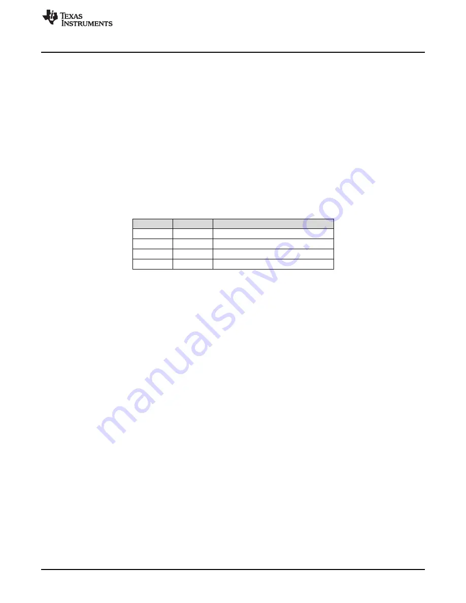
Table 12-2. I/O Function Selection
PxSEL1
PxSEL0
I/O Function
0
0
General purpose I/O is selected
0
1
Primary module function is selected
1
0
Secondary module function is selected
1
1
Tertiary module function is selected
Setting the PxSEL1 or PxSEL0 bits to a module function does not automatically set the pin direction.
Other peripheral module functions may require the PxDIR bits to be configured according to the direction
needed for the module function. See the pin schematics in the device-specific data sheet.
When a port pin is selected as an input to peripheral modules, the input signal to those peripheral
modules is a latched representation of the signal at the device pin. While PxSEL1 and PxSEL0 is other
than 00, the internal input signal follows the signal at the pin for all connected modules. However, if
PxSEL1 and PxSEL0 = 00, the input to the peripherals maintain the value of the input signal at the device
pin before the PxSEL1 and PxSEL0 bits were reset.
Because the PxSEL1 and PxSEL0 bits do not reside in contiguous addresses, changing both bits at the
same time is not possible. For example, an application might need to change P1.0 from general purpose
I/O to the tertiary module function residing on P1.0. Initially, P1SEL1 = 00h and P1SEL0 = 00h. To change
the function, it would be necessary to write both P1SEL1 = 01h and P1SEL0 = 01h. This is not possible
without first passing through an intermediate configuration, and this configuration may not be desirable
from an application standpoint. The PxSELC complement register can be used to handle such situations.
The PxSELC register always reads 0. Each set bit of the PxSELC register complements the
corresponding respective bit of the PxSEL1 and PxSEL0 registers. In the example, with P1SEL1 = 00h
and P1SEL0 = 00h initially, writing P1SELC = 01h causes P1SEL1 = 01h and P1SEL0 = 01h to be written
simultaneously.
12.2.7 Port Interrupts
All Px interrupt flags for a particular port are prioritized, with PxIFG.0 being the highest, and combined to
source a single interrupt vector. The highest priority enabled interrupt generates a number in the PxIV
register. This number can be evaluated or added to the program counter to automatically enter the
appropriate software routine. Disabled Px interrupts do not affect the PxIV value. The PxIV registers are
half-word access only.
Each PxIFG bit is the interrupt flag for its corresponding I/O pin, and the flag is set when the selected
input signal edge occurs at the pin. All PxIFG interrupt flags request an interrupt when their corresponding
PxIE bit is set. Software can also set each PxIFG flag, providing a way to generate a software-initiated
interrupt.
•
Bit = 0: No interrupt is pending


