


General-purpose timer (TIM2)
RM0453
846/1454
RM0453 Rev 2
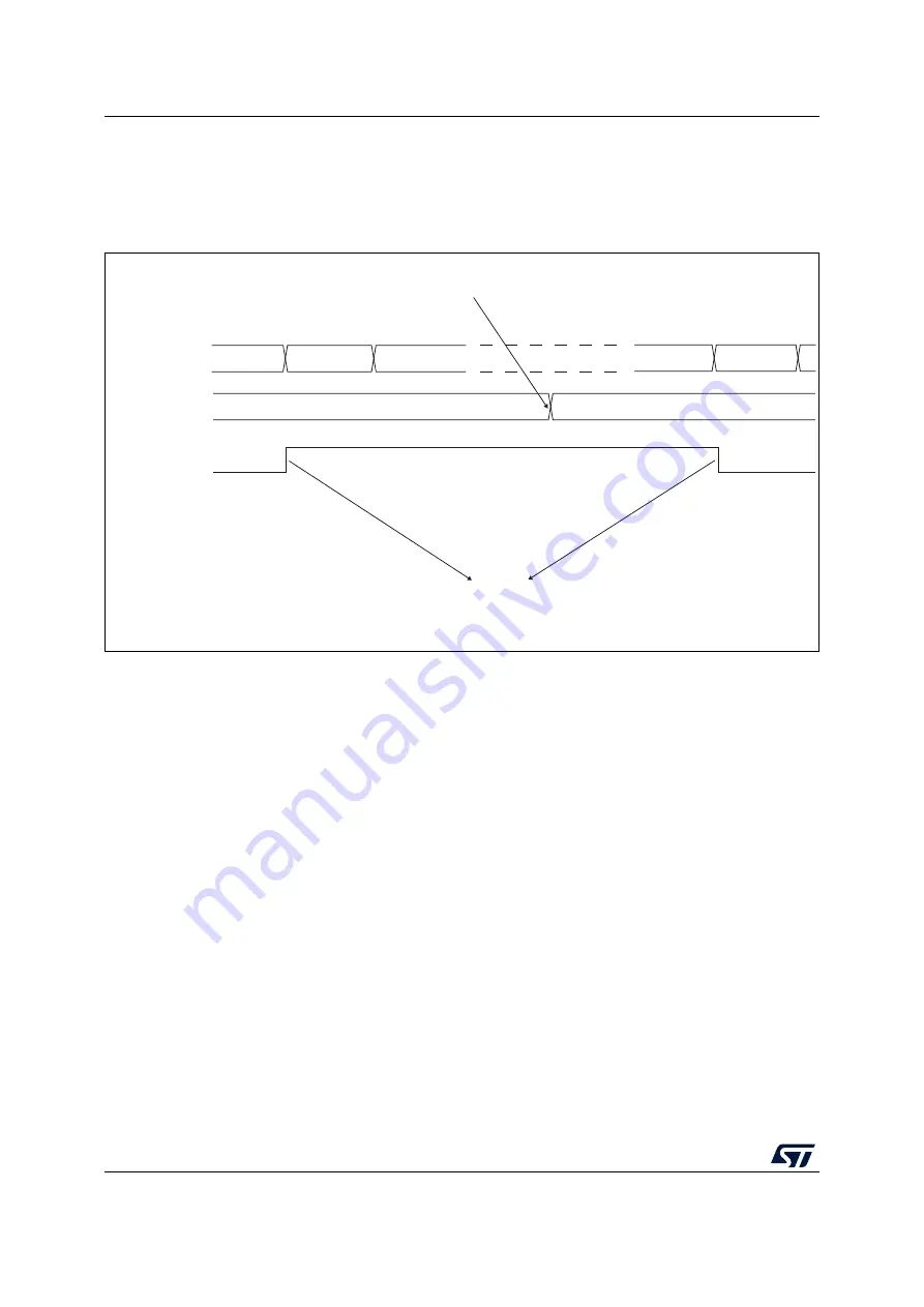
The TIMx_CCRx register can be updated at any time by software to control the output
waveform, provided that the preload register is not enabled (OCxPE=0, else TIMx_CCRx
shadow register is updated only at the next update event UEV). An example is given in
Figure 217. Output compare mode, toggle on OC1
26.3.9 PWM
mode
Pulse width modulation mode permits to generate a signal with a frequency determined by
the value of the TIMx_ARR register and a duty cycle determined by the value of the
TIMx_CCRx register.
The PWM mode can be selected independently on each channel (one PWM per OCx
output) by writing 110 (PWM mode 1) or ‘111 (PWM mode 2) in the OCxM bits in the
TIMx_CCMRx register. The corresponding preload register must be enabled by setting the
OCxPE bit in the TIMx_CCMRx register, and eventually the auto-reload preload register (in
upcounting or center-aligned modes) by setting the ARPE bit in the TIMx_CR1 register.
As the preload registers are transferred to the shadow registers only when an update event
occurs, before starting the counter, all registers must be initialized by setting the UG bit in
the TIMx_EGR register.
OCx polarity is software programmable using the CCxP bit in the TIMx_CCER register. It
can be programmed as active high or active low. OCx output is enabled by the CCxE bit in
the TIMx_CCER register. Refer to the TIMx_CCERx register description for more details.
In PWM mode (1 or 2), TIMx_CNT and TIMx_CCRx are always compared to determine
whether TIMx_CCRx
≤
TIMx_CNT or TIMx_CNT
≤
TIMx_CCRx (depending on the direction
of the counter). However, to comply with the OCREF_CLR functionality (OCREF can be
MS31092V1
OC1REF= OC1
TIM1_CNT
B200
B201
0039
TIM1_CCR1
003A
Write B201h in the CC1R register
Match detected on CCR1
Interrupt generated if enabled
003B
B201
003A