Module Descriptions, RFL 9508D Digital Section
8.1.2
8.1.3
T1/E1 LINE INTERFACE
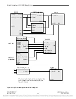
The CM4 receives its T1/E1 line input from a Module Adapter in 9508D chassis with electrical T1/E1
interfaces, or from an OIA (optical interface adapter) in 9508D chassis with fiber optic T1/E1
interfaces. The line coding can be either B8ZS/HDB3 or AMI.
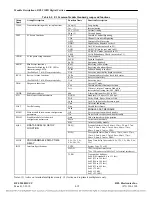
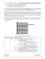
Equipment and monitor test jacks on the front of the Common Module accept miniature bantam plugs.
Plugging a T1/E1 transmission test set or the output of another 9508D chassis into the "T1/E1 EQUIP
IN" jack breaks the connection to the incoming T1/E1 line. The terminating impedance should be 100
ohms (balanced). The "T1/E1 MON IN" jack permits test access to the line input without breaking the
T1/E1 line connection. Equipment connected to this jack should also provide a 100 ohm termination
impedance. The signal level at this point is approximately 20 dB below the input.
The test jacks handle the T1/E1 signal originating or terminating at the module on which they are
located.
The line receiver accepts the input signal, recovers receive timing, and decodes the bipolar signal. A
jitter buffer is used to smooth out the timing jitter usually present on incoming signals.
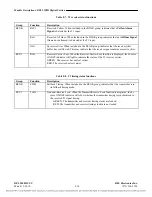
The T1/E1 line output connection is made through a Module Adapter in 9508D chassis with electrical
T1/E1 interfaces, or from the OIA in 9508D chassis with fiber optic interfaces. The “T1/E1 EQUIP
OUT” and “T1/E1 MON OUT” jacks function like the input test jacks described above. All equipment
connected to them should provide 100 ohms of termination. The “T1/E1 EQUIP OUT” jack breaks the
connection to the T1/E1 line output. The “T1/E1 MON OUT” jack does not break the connection, but
the signal level at this jack is about 20 dB below the output level.
T1/E1 MULTIPLEXING/DEMULTIPLEXING
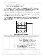
The decoded line receive signal feeds the demultiplexer circuitry where it achieves frame
synchronization. The mean time to lose frame in the presence of a high random bit error rate (10
-3
)
exceeds several hours.
Once frame synchronization is achieved, the demultiplexer develops the proper demultiplexer bus
signals and feeds them to all the channels cards plugged into the shelf. Bus signals include
demultiplexed channel data, demultiplexer synchronization status, and synchronization signals
necessary for proper decoding by the channel modules.
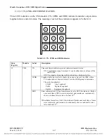
The CM4 develops backplane bus synchronization signals. The transmit section of each channel
module synchronizes to these signals, and places its data onto the selected bus. The CM4 then forms
the aggregate signal, using the selected framing format.
RFL 9508D UCC
RFL Electronics Inc.
March 11, 2010
8-4
(973) 334-3100

