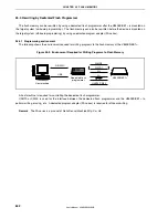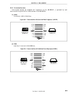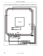
CHAPTER 26 FLASH MEMORY
User’s Manual U16896EJ2V0UD
642
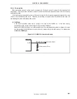
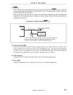
(2) FLMD1 pin
When 0 V is input to the FLMD0 pin, the FLMD1 pin does not function. When V
DD
is supplied to the FLMD0
pin, the flash memory programming mode is entered, so 0 V must be input to the FLMD1 pin. The following
shows an example of the connection of the FLMD1 pin.
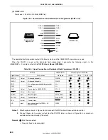
Figure 26-11. FLMD1 Pin Connection Example
FLMD1
Pull-down resistor (R
FLMD1
)
Other device
V850ES/KE1+
Caution If the V
DD
signal is input to the FLMD1 pin from another device during on-board writing and
immediately after reset, isolate this signal.
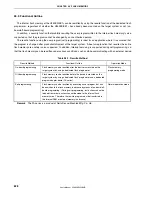
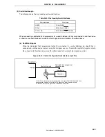
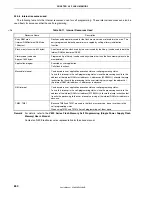
Table 26-8. Relationship Between FLMD0 and FLMD1 Pins and Operation Mode When Reset Is Released
FLMD0 FLMD1
Operation
Mode
0
don’t care
Normal operation mode
V
DD
0
Flash memory programming mode
V
DD
V
DD
Setting
prohibited
Содержание ?PD703302
Страница 2: ...User s Manual U16896EJ2V0UD 2 MEMO ...

