CHAPTER 13 A/D CONVERTER
User’s Manual U16896EJ2V0UD
372
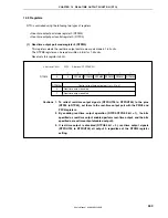
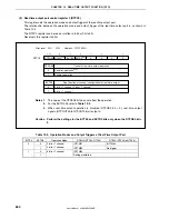
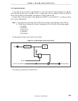
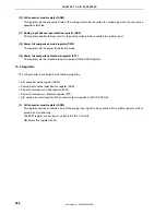
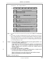
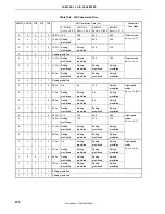
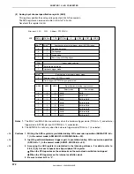
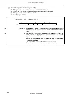
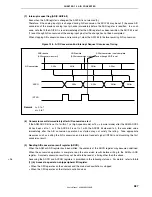
(2) Analog input channel specification register (ADS)
This register specifies the analog voltage input port for A/D conversion.
The ADS register can be read or written in 8-bit or 1-bit units.
Reset sets this register to 00H.
EGA1
Note 1
ADS
EGA0
Note 1
TRG
ADTMD
Note 2
0
ADS2
ADS1
ADS0
ANI0
ANI1
ANI2
ANI3
ANI4
ANI5
ANI6
ANI7
ANI0
ANI0, ANI1
ANI0 to ANI2
ANI0 to ANI3
ANI0 to ANI4
ANI0 to ANI5
ANI0 to ANI6
ANI0 to ANI7
ADS2
0
0
0
0
1
1
1
1
ADS1
0
0
1
1
0
0
1
1
ADS0
0
1
0
1
0
1
0
1
Specification of analog input channel
Select mode
Scan mode
No edge detection
Falling edge
Rising edge
Both rising and falling edges
EGA1
Note 1
0
0
1
1
EGA0
Note 1
0
1
0
1
Specification of external trigger signal (ADTRG) edge
After reset: 00H R/W Address: FFFFF201H
TRG
0
1
Software trigger mode
Hardware trigger mode
Trigger mode selection
ADTMD
Note 2
0
1
External trigger (ADTRG pin input)
Timer trigger (INTTM010 signal generated)
Specification of hardware trigger mode
Notes 1.
The EGA1 and EGA0 bits are valid only when the hardware trigger mode (TRG bit = 1) and external
trigger mode (ADTRG pin input: ADTMD bit = 1) are selected.
2.
The ADTMD bit is valid only when the hardware trigger mode (TRG bit = 1) is selected.
Cautions 1. Writing the ADS register is prohibited during A/D conversion operation (ADM.ADCS bit =
1) in the normal mode (ADM.ADHS1, ADM.ADHS0 bits = 00).
2. Inputting software/hardware trigger again is prohibited during A/D conversion operation
(ADCS bit = 1) in the normal mode (ADHS1, ADHS0 bits = 00).
3. Accessing the ADS register is prohibited in the following statuses. For details, refer to
3.4.8 (1) (b) Access to special on-chip peripheral I/O register.
•
When the CPU operates on the subclock and the main clock oscillation is stopped
•
When the CPU operates on the internal oscillation clock
4. Be sure to clear bit 3 to “0”.
<R>
<R>
<R>
Содержание ?PD703302
Страница 2: ...User s Manual U16896EJ2V0UD 2 MEMO ...


