


CHAPTER 26 FLASH MEMORY
User’s Manual U16896EJ2V0UD
634
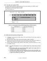
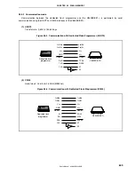
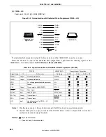
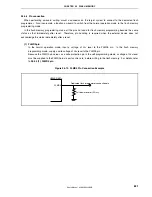
(3) CSI00 + HS
Serial clock: 2.4 kHz to 2.5 MHz (MSB first)
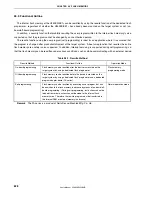
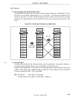
Figure 26-5. Communication with Dedicated Flash Programmer (CSI00 + HS)
Dedicated flash
programmer
V850ES/KE1+
V
DD
V
SS
RESET
SO00
SI00
SCK00
PCM0
V
DD
FLMD1
FLMD1
FLMD0
FLMD0
GND
RESET
SI
SO
SCK
HS
PG-FP4
(Flash Pro4)
Cxxxxxx
Bxxxxx
Axxxx
X
X
X
Y
Y
Y
X
X
X
X
X
X
X
X
X
X
X
X
X
X
X
X
X
X
X Y
Y
Y
Y
STATVE
X1
X2
CLK
The dedicated flash programmer outputs the transfer clock, and the V850ES/KE1+ operates as a slave.
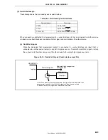
When the PG-FP4 is used as the dedicated flash programmer, it generates the following signals to the
V850ES/KE1+. For details, refer to the
PG-FP4 User’s Manual (U15260E)
.
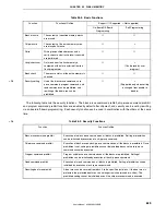
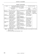
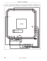
Table 26-5. Signal Connections of Dedicated Flash Programmer (PG-FP4)
PG-FP4
V850ES/KE1+
Processing for Connection
Signal Name
I/O
Pin Function
Pin Name
UART0
CSI00
CSI00 + HS
FLMD0 Output
Write
enable/disable
FLMD0
FLMD1 Output
Write
enable/disable
FLMD1
Note 1
Note 1
Note 1
VDD
−
V
DD
voltage generation/voltage monitor
V
DD
GND
−
Ground V
SS
CLK
Output
Clock output to V850ES/KE1+
X1, X2
×
Note 2
×
Note 2
×
Note 2
RESET Output
Reset
signal
RESET
SI/RxD Input
Receive
signal
SO00,
TXD0
SO/TxD
Output
Transmit signal
SI00, RXD0
SCK Output
Transfer
clock
SCK00
×
HS Input
Handshake signal for CSI00 + HS
communication
PCM0
×
×
Notes 1.
Wire the pin as shown in Figure 26-6, or connect it to GND on board via a pull-down resistor.
2.
Connect these pins to supply a clock from the PG-FP4 (wire as shown in Figure 26-6, or create an
oscillator on board and supply the clock).
Remark
: Must be connected.
×
: Does not have to be connected.
Содержание ?PD703302
Страница 2: ...User s Manual U16896EJ2V0UD 2 MEMO ...