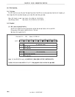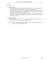
CHAPTER
4 P
O
RT
FU
NCTI
O
NS
User’s Manual
U1
6896EJ2V0UD
120
Other Bits (Registers)
–
–
–
–
–
–
–
–
–
–
–
–
–
–
–
–
–
–
–
PFCnx Bit of PFCn
Register
–
–
–
PFC03 = 0
–
–
–
PFC30 = 0
Note 1
, PFC31 = 0
Note 1
, PFC31 = 0
Note 2
, PFC32 = 0
Note 2
, PFC32 = 0
PFC32 = 1
PFC33 = 0
PFC33 = 1
PFC34 = 0
PFC34 = 1
PFC35 = 0
PFC35 = 1
PFCEnx Bit of
PFCEn Register
–
–
–
–
–
–
–
–
–
–
–
–
–
PFCE33 = 1
PFCE33 = 1
PFCE34 = 1
PFCE34 = 1
–
–
PMCnx Bit of
PMCn Register
PMC00 = 1
PMC01 = 1
PMC02 = 1
PMC03 = 1
PMC04 = 1
PMC05 = 1
PMC06 = 1
PMC30 = 1
PMC31 = 1
PMC31 = 1
PMC32 = 1
PMC32 = 1
PMC32 = 1
PMC33 = 1
PMC33 = 1
PMC34 = 1
PMC34 = 1
PMC35 = 1
PMC35 = 1
PMnx Bit of PMn Register
PM00 = Setting not required
PM01 = Setting not required
PM02 = Setting not required
PM03 = Setting not required
PM04 = Setting not required
PM05 = Setting not required
PM06 = Setting not required
PM30 = Setting not required
PM31 = Setting not required
PM31 = Setting not required
PM32 = Setting not required
PM32 = Setting not required
PM32 = Setting not required
PM33 = Setting not required
PM33 = Setting not required
PM34 = Setting not required
PM34 = Setting not required
PM35 = Setting not required
PM35 = Setting not required
Pnx Bit of Pn Register
P00 = Setting not required
P01 = Setting not required
P02 = Setting not required
P03 = Setting not required
P04 = Setting not required
P05 = Setting not required
P06 = Setting not required
P30 = Setting not required
P31 = Setting not required
P31 = Setting not required
P32 = Setting not required
P32 = Setting not required
P32 = Setting not required
P33 = Setting not required
P33 = Setting not required
P34 = Setting not required
P34 = Setting not required
P35 = Setting not required
P35 = Setting not required
I/O
Output
Output
Input
Input
Input
Input
Input
Output
Input
Input
Input
Input
Output
Input
Output
Input
Output
Input
Output
Alternate Function
Function Name
TOH0
TOH1
NMI
INTP0
INTP1
INTP2
INTP3
TXD0
RXD0
INTP7
ASCK0
ADTRG
TO01
TIP00
TOP00
TIP10
TOP10
TI010
TO01
Table 4-12. Settings When Port Pins Are Used for Alternate Functions (1/3)
Pin Name
P00
P01
P02
P03
P04
P05
P06
P30
P31
P32
P33
P34
P35
Notes 1.
The INTP7 and RXD0 pins are alternate-function pins. When using the pin as the RXD0 pin, disable edge detection of the alternate-function INTP7 pin (clear
the INTF3.INTF31 and INTR3.INTR31 bits to 0). When using the pin as the INTP7 pin, stop the UART0 receive operation (clear the ASIM0.RXE0 bit to 0).
2.
The ASCK0 and ADTRG pins are alternate-function pins. When using the pin as the ASCK0 pin, disable the trigger input of the alternate-function ADTRG pin
(clear the ADS.TRG bit to 0 or set the ADS.ADTMD bit to 1). When using the pin as the ADTRG pin, do not set the UART0 operation clock to external input
(set the CKSR0.TPS03 to CKSR0.TPS00 bits to other than 1011).
Содержание ?PD703302
Страница 2: ...User s Manual U16896EJ2V0UD 2 MEMO ...

