


User’s Manual U16896EJ2V0UD
32
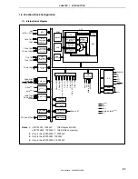
CHAPTER 2 PIN FUNCTIONS
The names and functions of the pins of the V850ES/KE1+ are described below, divided into port pins and non-port
pins.
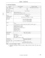
The pin I/O buffer power supplies are divided into two systems; AV
REF0
and EV
DD
. The relationship between these
power supplies and the pins is shown below.
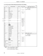
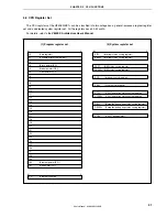
Table 2-1. Pin I/O Buffer Power Supplies
Power Supply
Corresponding Pins
AV
REF0
Port
7
EV
DD
RESET, ports 0, 3 to 5, 9, CM, DL
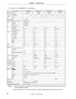
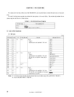
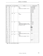
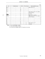
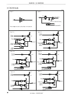
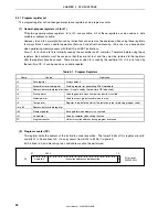
2.1 List of Pin Functions
(1) Port
pins
(1/2)
Pin Name Pin No.
I/O
Pull-up Resistor
Function Alternate
Function
P00 12
TOH0
P01 13
TOH1
P02 14
NMI
P03 15
INTP0
P04 16
INTP1
P05 17
INTP2
P06 18
I/O Yes
Port 0
I/O port
Input/output can be specified in 1-bit units.
INTP3
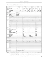
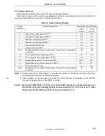
P30 22
TXD0
P31 23
RXD0/INTP7
P32 24
ASCK0/ADTRG/TO01
P33 25
TIP00/TOP00
P34 26
TIP01/TOP01
P35 27
Yes
TI010/TO01
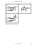
P38 55
SDA0
Note 2
P39 56
I/O
No
Note 1
Port 3
I/O port
Input/output can be specified in 1-bit units.
P38 and P39 are fixed to N-ch open-drain
output.
SCL0
Note 2
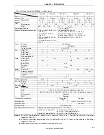
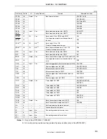
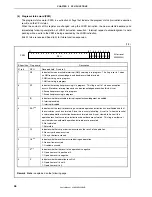
P40 19
SI00
P41 20
SO00
P42 21
I/O Yes
Port 4
I/O port
Input/output can be specified in 1-bit units.
P41 and P42 can be specified as N-ch open-
drain output in 1-bit units.
SCK00
Notes 1.
An on-chip pull-up resistor can be provided by a mask option (only in the
μ
PD703302, 703302Y).
2.
Only in the
μ
PD703302Y, 70F3302Y
Содержание ?PD703302
Страница 2: ...User s Manual U16896EJ2V0UD 2 MEMO ...