CHAPTER 15 CLOCKED SERIAL INTERFACE 0 (CSI0)
User’s Manual U16896EJ2V0UD
437
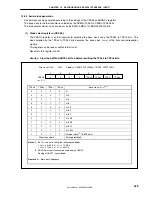
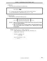
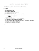
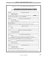
<7>
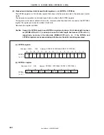
CSI0En
CSIM0n
(n = 0, 1)
<6>
TRMDn
5
CCLn
<4>
DIRn
3
CSITn
2
AUTOn
1
0
<0>
CSOTn
After reset: 00H R/W Address: CSIM00 FFFFFD00H, CSIM01 FFFFFD10H
CSI0En
CSI0n operation enable/disable
0
Disable CSI0n operation.
1
Enable CSI0n operation.
The internal CSI0n circuit can be reset
Note
asynchronously by clearing the CSI0En bit to 0. For the SCK0n and SO0n
pin output status when the CSI0En bit = 0, refer to
15.5 Output Pins
.
TRMDn
Specification of transmission/reception mode
0 Receive-only
mode
1 Transmission/reception
mode
When the TRMDn bit = 0, reception is performed and the SO0n pin outputs a low level. Data reception is started by
reading the SIRBn register.
When the TRMDn bit = 1, transmission/reception is started by writing data to the SOTBn register.
CCLn
Specification of data length
0 8
bits
1 16
bits
DIRn
Specification of transfer direction mode (MSB/LSB)
0
First bit of transfer data is MSB
1
First bit of transfer data is LSB
CSITn
Control of delay of interrupt request signal
0 No
delay
1
Delay mode (interrupt request signal is delayed 1/2 cycle compared to the serial clock)
The delay mode (CSITn bit = 1) is valid only in the master mode (CSICn.CKS0n2 to CSICn.CKS0n0 bits are not
111B). In the slave mode (CKS0n2 to CKS0n0 bits are 111B), do not set the delay mode.
AUTOn
Specification of single transfer mode or continuous transfer mode
0
Single transfer mode
1
Continuous transfer mode
CSOTn Communication
status
flag
0 Communication
stopped
1
Communication in progress
The CSOTn bit is cleared (0) by writing 0 to the CSI0En bit.
Note
The CSOTn bit and the SIRBn, SIRBnL, SIRBE, SIRBEnL, SIOn, and SIOnL registers are reset.
Содержание ?PD703302
Страница 2: ...User s Manual U16896EJ2V0UD 2 MEMO ...

