CHAPTER 6 16-BIT TIMER/EVENT COUNTER P (TMP)
User’s Manual U16896EJ2V0UD
172
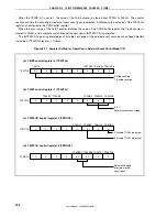
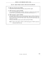
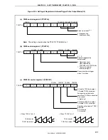
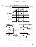
Figure 6-18. Setting of Registers in External Trigger Pulse Output Mode (2/2)
(d) TMP0 I/O control register 2 (TP0IOC2)
0
0
0
0
0/1
TP0IOC2
Select valid edge of
external trigger input
Select valid edge of
external event count input
0/1
0/1
0/1
TP0EES0 TP0ETS1 TP0ETS0
TP0EES1
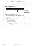
(e) TMP0 counter read buffer register (TP0CNT)
The value of the 16-bit counter can be read by reading the TP0CNT register.
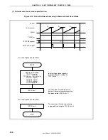
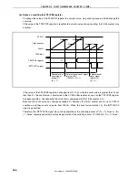
(f) TMP0 capture/compare registers 0 and 1 (TP0CCR0 and TP0CCR1)
If D
0
is set to the TP0CCR0 register and D
1
to the TP0CCR1 register, the cycle and active level width of
the PWM waveform are as follows.
Cycle = (D
0
+ 1)
×
Count clock cycle
Active level width = D
1
×
Count clock cycle
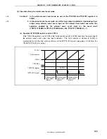
Remark
TMP0 I/O control register 1 (TP0IOC1) and TMP0 option register 0 (TP0OPT0) are not used
in the external trigger pulse output mode.
Содержание ?PD703302
Страница 2: ...User s Manual U16896EJ2V0UD 2 MEMO ...


