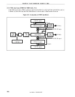
CHAPTER 6 16-BIT TIMER/EVENT COUNTER P (TMP)
User’s Manual U16896EJ2V0UD
194
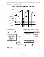
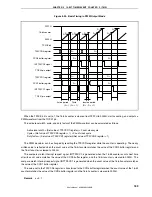
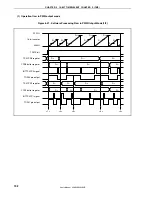
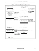
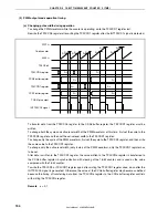
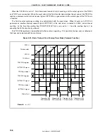
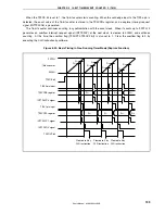
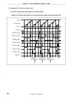
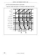
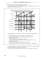
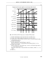
(2) PWM output mode operation timing
(a) Changing pulse width during operation
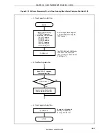
To change the PWM waveform while the counter is operating, write the TP0CCR1 register last.
Rewrite the TP0CCRa register after writing the TP0CCR1 register after the INTTP0CC1 signal is detected.
FFFFH
16-bit counter
0000H
TP0CE bit
TP0CCR0 register
CCR0 buffer register
TP0CCR1 register
CCR1 buffer register
TOP01 pin output
INTTP0CC0 signal
D
10
D
00
D
00
D
01
D
00
D
10
D
11
D
10
D
11
D
01
D
10
D
10
D
00
D
00
D
11
D
11
D
01
D
01
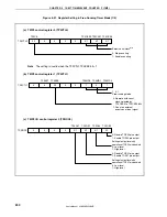
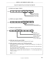
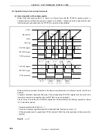
To transfer data from the TP0CCRa register to the CCRa buffer register, the TP0CCR1 register must be
written.
To change both the cycle and active level width of the PWM waveform at this time, first set the cycle to the
TP0CCR0 register and then set the active level width to the TP0CCR1 register.
To change only the cycle of the PWM waveform, first set the cycle to the TP0CCR0 register, and then write
the same value to the TP0CCR1 register.
To change only the active level width (duty factor) of the PWM waveform, only the TP0CCR1 register has
to be set.
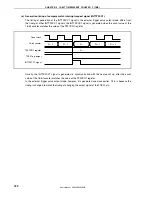
After data is written to the TP0CCR1 register, the value written to the TP0CCRa register is transferred to
the CCRa buffer register in synchronization with clearing of the 16-bit counter, and is used as the value
compared with the 16-bit counter.
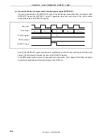
To write the TP0CCR0 or TP0CCR1 register again after writing the TP0CCR1 register once, do so after the
INTTP0CC0 signal is generated. Otherwise, the value of the CCRa buffer register may become undefined
because the timing of transferring data from the TP0CCRa register to the CCRa buffer register conflicts
with writing the TP0CCRa register.
Remark
a = 0, 1
Содержание ?PD703302
Страница 2: ...User s Manual U16896EJ2V0UD 2 MEMO ...

