CHAPTER 16 I
2
C BUS
User’s Manual U16896EJ2V0UD
466
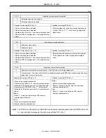
(2/4)
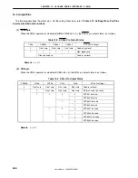
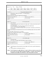
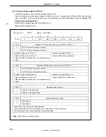
SPIE0
Note
Enable/disable generation of interrupt request when stop condition is detected
0 Disable
1 Enable
Condition for clearing (SPIE0 bit = 0)
Condition for setting (SPIE0 bit = 1)
•
Cleared by instruction
•
Reset
•
Set by instruction
WTIM0
Note
Control of wait and interrupt request generation
0
Interrupt request is generated at the eighth clock’s falling edge.
Master mode: After output of eight clocks, clock output is set to low level and wait is set.
Slave mode: After input of eight clocks, the clock is set to low level and wait is set for master device.
1
Interrupt request is generated at the ninth clock’s falling edge.
Master mode: After output of nine clocks, clock output is set to low level and wait is set.
Slave mode: After input of nine clocks, the clock is set to low level and wait is set for master device.
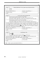
An interrupt is generated at the falling edge of the ninth clock during address transfer independently of the setting of this
bit. The setting of this bit is valid when the address transfer is completed. When in master mode, a wait is inserted at
the falling edge of the ninth clock during address transfers. For a slave device that has received a local address, a wait
is inserted at the falling edge of the ninth clock after ACK is issued. However, when the slave device has received an
extension code, a wait is inserted at the falling edge of the eighth clock.
Condition for clearing (WTIM0 bit = 0)
Condition for setting (WTIM0 bit = 1)
•
Cleared by instruction
•
Reset
•
Set by instruction
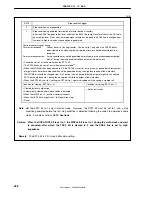
ACKE0
Note
Acknowledgment
control
0 Disable
ACK.
1
Enable ACK. During the ninth clock period, the SDA0 line is set to low level.
The ACKE0 bit setting is invalid for address reception. In this case, ACK is generated when the addresses match.
However, the ACKE0 bit setting is valid for address reception of the extension code.
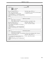
Condition for clearing (ACKE0 bit = 0)
Condition for setting (ACKE0 bit = 1)
•
Cleared by instruction
•
Reset
•
Set by instruction
Note
This flag’s signal is invalid when the IICE0 bit = 0.
Содержание ?PD703302
Страница 2: ...User s Manual U16896EJ2V0UD 2 MEMO ...

