CHAPTER 26 FLASH MEMORY
User’s Manual U16896EJ2V0UD
649
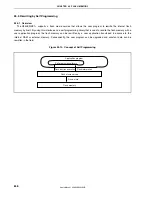
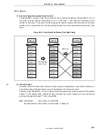
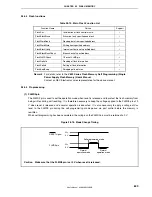
26.5.4 Flash functions
Table 26-10. Main Flash Function List
Function Name
Outline
Support
FlashEnv Initialization
of flash control macro
√
FlashBlockErase
Erasure of only specified one block
√
FlashWordRead
Reading data from specified address
√
FlashWordWrite
Writing from specified address
√
FlashBlockIVerify
Internal verification of specified block
√
FlashBlockBlankCheck
Blank check of specified block
√
FlashFLMDCheck
Check of FLMD pin
√
FlashGetInfo
Reading of flash information
√
FlashSetInfo
Setting of flash information
√
FlashBootSwap
Swapping of boot area
√
Remark
For details, refer to the
V850 Series Flash Memory Self Programming (Single
Power Supply Flash Memory) User’s Manual
.
Contact an NEC Electronics sales representative for the above manual.
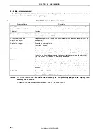
26.5.5 Pin processing
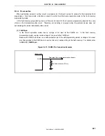
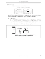
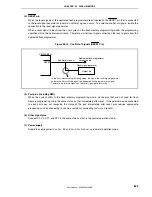
(1) FLMD0 pin
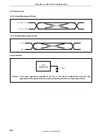
The FLMD0 pin is used to set the operation mode when reset is released and to protect the flash memory from
being written during self rewriting. It is therefore necessary to keep the voltage applied to the FLMD0 pin at 0
V when reset is released and a normal operation is executed. It is also necessary to apply a voltage of V
DD
level to the FLMD0 pin during the self programming mode period via port control before the memory is
rewritten.
When self programming has been completed, the voltage on the FLMD0 pin must be returned to 0 V.
Figure 26-18. Mode Change Timing
RESET signal
FLMD0 pin
V
DD
0 V
V
DD
0 V
Self programming mode
Normal
operation mode
Normal
operation mode
Caution Make sure that the FLMD0 pin is at 0 V when reset is released.
Содержание ?PD703302
Страница 2: ...User s Manual U16896EJ2V0UD 2 MEMO ...


