10 INPUT/OUTPUT PORT (P)
84
EPSON
S1C17001 TECHNICAL MANUAL
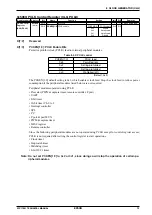
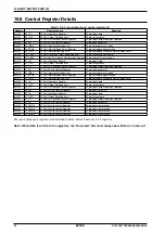
10.2 Input/Output Pin Function Selection (Port MUX)
The input/output port pins share peripheral module input/output pins (with certain exceptions). Each pin can be set
for use as an input/output port or for peripheral modules via the corresponding port function selection bits for each
port. Pins not used for peripheral modules can be used as general purpose input/output ports.
Table 10.2.1: Input/output pin function selection
Pin function 1
P
xx
MUX = 0
Pin function 2
P
xx
MUX = 1
Port function
selection bit
Control register
P00
–
–
–
P01
–
–
–
P02
–
–
–
P03
–
–
–
P04
REMI (REMC)
P04MUX (D4) P0 Port Function Select (P0_PMUX) Register (0x52a0)
P05
REMO (REMC)
P05MUX (D5)
P06/EXCL2
(T16CH2) –
–
–
P07/EXCL1
(T16CH1) –
–
–
P10
–
–
–
P11
–
–
–
P12
–
–
–
P13
FOUT1 (OSC)
P13MUX (D3) P1 Port Function Select (P1_PMUX) Register (0x52a1)
P14
SDA (I2C)
P14MUX (D4)
P15
SCL (I2C)
P15MUX (D5)
P16/EXCL0
(T16CH0) –
–
–
P17
#SPISS (SPI)
P17MUX (D7) P1 Port Function Select (P1_PMUX) Register (0x52a1)
P20
SDI (SPI)
P20MUX (D0) P2 Port Function Select (P2_PMUX) Register (0x52a2)
P21
SDO (SPI)
P21MUX (D1)
P22
SPICLK (SPI)
P22MUX (D2)
P23
SIN (UART)
P23MUX (D3)
P24
SOUT (UART)
P24MUX (D4)
P25
SCLK (UART)
P25MUX (D5)
P26
TOUT (T16E)
P26MUX (D6)
P27
EXCL3 (T16E)
P27MUX (D7)
P30
FOUT3 (OSC)
P30MUX (D0) P3 Port Function Select (P3_PMUX) Register (0x52a3)
DCLK
(DBG)
P31
P31MUX (D1)
DST2
(DBG)
P32
P32MUX (D2)
DSIO
(DBG)
P33
P33MUX (D3)
Resetting the input/output port pins (P
xx
) resets them to their default functions (pin function 1 in Table 10.2.1).
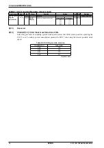
Pins P06, P07, and P16 can also be used as 16-bit timer external clock input pins by setting them to input mode.
Note, however, that no port function selection bits are available, since they are simultaneously set to function as
general purpose input ports.
For information on functions other than the input/output ports, refer to the discussion of the peripheral modules in-
dicated in parentheses. The sections below discuss port functions with the pins set as general purpose input/output
ports.
Содержание S1C17001
Страница 1: ...Technical Manual S1C17001 CMOS 16 BIT SINGLE CHIP MICROCONTROLLER ...
Страница 31: ...3 MEMORY MAP AND BUS CONTROL 22 EPSON S1C17001 TECHNICAL MANUAL This page intentionally left blank ...
Страница 33: ...4 POWER SUPPLY VOLTAGE 24 EPSON S1C17001 TECHNICAL MANUAL This page intentionally left blank ...
Страница 63: ...6 INITERRUPT CONTROLLER 54 EPSON S1C17001 TECHNICAL MANUAL This page intentionally left blank ...
Страница 87: ...8 CLOCK GENERATOR CLG 78 EPSON S1C17001 TECHNICAL MANUAL This page intentionally left blank ...
Страница 91: ...9 PRESCALER PSC 82 EPSON S1C17001 TECHNICAL MANUAL This page intentionally left blank ...
Страница 133: ...11 16 BIT TIMER T16 124 EPSON S1C17001 TECHNICAL MANUAL This page intentionally left blank ...
Страница 185: ...14 8 BIT OSC1 TIMER T8OSC1 176 EPSON S1C17001 TECHNICAL MANUAL This page intentionally left blank ...
Страница 211: ...16 STOPWATCH TIMER SWT 202 EPSON S1C17001 TECHNICAL MANUAL This page intentionally left blank ...
Страница 219: ...17 WATCHDOG TIMER WDT 210 EPSON S1C17001 TECHNICAL MANUAL This page intentionally left blank ...
Страница 241: ...18 UART 232 EPSON S1C17001 TECHNICAL MANUAL This page intentionally left blank ...
Страница 277: ...20 I2 C 268 EPSON S1C17001 TECHNICAL MANUAL This page intentionally left blank ...
Страница 297: ...21 REMOTE CONTROLLER REMC 288 EPSON S1C17001 TECHNICAL MANUAL This page intentionally left blank ...
Страница 303: ...22 ON CHIP DEBUGGER DBG 294 EPSON S1C17001 TECHNICAL MANUAL This page intentionally left blank ...
Страница 313: ...25 PACKAGE 304 EPSON S1C17001 TECHNICAL MANUAL This page intentionally left blank ...

