22 ON-CHIP DEBUGGER (DBG)
S1C17001 TECHNICAL MANUAL
EPSON
289
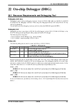
22 On-chip Debugger (DBG)
22.1 Resource Requirements and Debugging Tool
Debugging work area
Debugging requires a 64-byte debugging work area. In the S1C17001, RAM addresses 0x0007c0 to 0x0007ff
are assigned as the debugging work area. When using the debugging function, avoid using this area for any
other user applications.
The start address for this debugging work area can be read from the DBRAM register (0xffff90).
Debugging tool
Debugging involves connecting an ICD (In-Circuit Debugger) such as S5U1C17001H (ICD Mini) to the
S1C17701 debug pin and inputting the debug command from the PC debugger.
The following tools are required:
• S1C17 Family In-Circuit Debugger (e.g., S5U1C17001H)
• S1C17 Family C compiler package (S5U1C17001C)
Debug pins
The following debug pins are used to connect an ICD (e.g., S5U1C17001H).
Table 22.1.1: Debug pin list
Pin name
I/O
Qty
Function
DCLK (P31)
O
1
On-chip debugger clock output pin
Outputs a clock to the ICD.
DSIO (P33)
I/O
1
On-chip debugger data input/output pin
Used for inputting/outputting debugging data and inputting break signals.
DST2 (P32)
O
1
On-chip debugger status signal output pin
Outputs the processor status during debugging.
Shared with general purpose input/output port pins (P31, P32, P33), the on-chip debugger input/output pins
(DCLK, DST2, DSIO) are initially set for use as debugger pins. If the debugging function is not used, these
pins can be switched via the P3_PMUX register to enable use as general purpose input/output port pins. Set the
control bits shown below to 1 to switch the pins to general purpose input/output port use.
DCLK
→
P31
∗
P31MUX
: P31 Port Function Select Bit in the P3 Port Function Select (P3_PMUX) Register (D1/0x52a3)
DST2
→
P32
∗
P32MUX
: P32 Port Function Select Bit in the P3 Port Function Select (P3_PMUX) Register (D2/0x52a3)
DSIO
→
P33
∗
P33MUX
: P33 Port Function Select Bit in the P3 Port Function Select (P3_PMUX) Register (D3/0x52a3)
For more information on pin function and switching, refer to “10.2 Input/Output Pin Function Selection (Port
MUX).”
Содержание S1C17001
Страница 1: ...Technical Manual S1C17001 CMOS 16 BIT SINGLE CHIP MICROCONTROLLER ...
Страница 31: ...3 MEMORY MAP AND BUS CONTROL 22 EPSON S1C17001 TECHNICAL MANUAL This page intentionally left blank ...
Страница 33: ...4 POWER SUPPLY VOLTAGE 24 EPSON S1C17001 TECHNICAL MANUAL This page intentionally left blank ...
Страница 63: ...6 INITERRUPT CONTROLLER 54 EPSON S1C17001 TECHNICAL MANUAL This page intentionally left blank ...
Страница 87: ...8 CLOCK GENERATOR CLG 78 EPSON S1C17001 TECHNICAL MANUAL This page intentionally left blank ...
Страница 91: ...9 PRESCALER PSC 82 EPSON S1C17001 TECHNICAL MANUAL This page intentionally left blank ...
Страница 133: ...11 16 BIT TIMER T16 124 EPSON S1C17001 TECHNICAL MANUAL This page intentionally left blank ...
Страница 185: ...14 8 BIT OSC1 TIMER T8OSC1 176 EPSON S1C17001 TECHNICAL MANUAL This page intentionally left blank ...
Страница 211: ...16 STOPWATCH TIMER SWT 202 EPSON S1C17001 TECHNICAL MANUAL This page intentionally left blank ...
Страница 219: ...17 WATCHDOG TIMER WDT 210 EPSON S1C17001 TECHNICAL MANUAL This page intentionally left blank ...
Страница 241: ...18 UART 232 EPSON S1C17001 TECHNICAL MANUAL This page intentionally left blank ...
Страница 277: ...20 I2 C 268 EPSON S1C17001 TECHNICAL MANUAL This page intentionally left blank ...
Страница 297: ...21 REMOTE CONTROLLER REMC 288 EPSON S1C17001 TECHNICAL MANUAL This page intentionally left blank ...
Страница 303: ...22 ON CHIP DEBUGGER DBG 294 EPSON S1C17001 TECHNICAL MANUAL This page intentionally left blank ...
Страница 313: ...25 PACKAGE 304 EPSON S1C17001 TECHNICAL MANUAL This page intentionally left blank ...


