20 I
2
C
S1C17001 TECHNICAL MANUAL
EPSON
253
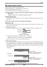
20.5 Data Transfer Control
Make the following settings before starting data transfers.
(1) Set the 16-bit timer Ch.2 to output the I
2
C clock. (See Section 11.)
(2) Select the option function. (See section 20.4.)
(3) Set the interrupt conditions to use I
2
C interrupts. (See Section 20.6.)
Note: Make sure the I
2
C module is halted (when I2CEN/I2C_EN register = 0) before changing the
above settings.
∗
I2CEN
: I
2
C Enable Bit in the I
2
C Enable (I2C_EN) Register (D0/0x4340)
Permitting data transfers
Set the I2CEN (D0/I2C_EN register) to 1 to permit I
2
C operations. This enables I
2
C transfers and permits clock
input/output.
Note: Do not set I2CEN to 0 when the I
2
C module is transferring data.
Data transfer start
To start data transfers, the I
2
C master (this module) must generate the start condition. The slave address is then
sent to establish communications.
(1) Generate start condition
The start condition applies when the SCL line is maintained at High and the SDA line is maintained at Low.
SDA (output)
SCL (output)
Start condition
Figure 20.5.1: Start condition
The start condition is generated by setting STRT (D0/I2C_CTL register) to 1.
∗
STRT
: Start Control Bit in the I
2
C Control (I2C_CTL) Register (D0/0x4342)
STRT is automatically reset to 0 once the start condition is generated.
(2) Slave address transmission
Once the start condition has been generated, the I
2
C master (this module) sends a bit indicating the slave ad-
dress and transfer direction for communications. I
2
C slave addresses are either 7-bit or 10-bit. This module uses
an 8-bit transfer data register to send the slave address and transfer direction bit, enabling single transfers in
7-bit address mode. In 10-bit mode, data is sent twice under software control. Figure 20.5.2 gives the configu-
ration of the address data.
Slave address
7-bit address
Transfer direction
0: Master
→
Slave (data transmission)
1: Slave
→
Master (date receipt)
A6
A5
D7
D6
A4
D5
A3
D4
A2
D3
A1
D2
A0
D1
DIR
D0
Slave address last 8 bits
A7
A6
D7
D6
A5
D5
A4
D4
A3
D3
A2
D2
A1
D1
A0
D0
Slave address
first 2 bits
10-bit address
Transfer direction
0: Master
→
Slave (data transmission)
1: Slave
→
Master (date receipt)
1
First data sent
Second data sent
1
D7
D6
1
D5
1
D4
0
D3
A9
D2
A8
D1
DIR
D0
Figure 20.5.2: Slave address and transmission data specifying transfer direction
Содержание S1C17001
Страница 1: ...Technical Manual S1C17001 CMOS 16 BIT SINGLE CHIP MICROCONTROLLER ...
Страница 31: ...3 MEMORY MAP AND BUS CONTROL 22 EPSON S1C17001 TECHNICAL MANUAL This page intentionally left blank ...
Страница 33: ...4 POWER SUPPLY VOLTAGE 24 EPSON S1C17001 TECHNICAL MANUAL This page intentionally left blank ...
Страница 63: ...6 INITERRUPT CONTROLLER 54 EPSON S1C17001 TECHNICAL MANUAL This page intentionally left blank ...
Страница 87: ...8 CLOCK GENERATOR CLG 78 EPSON S1C17001 TECHNICAL MANUAL This page intentionally left blank ...
Страница 91: ...9 PRESCALER PSC 82 EPSON S1C17001 TECHNICAL MANUAL This page intentionally left blank ...
Страница 133: ...11 16 BIT TIMER T16 124 EPSON S1C17001 TECHNICAL MANUAL This page intentionally left blank ...
Страница 185: ...14 8 BIT OSC1 TIMER T8OSC1 176 EPSON S1C17001 TECHNICAL MANUAL This page intentionally left blank ...
Страница 211: ...16 STOPWATCH TIMER SWT 202 EPSON S1C17001 TECHNICAL MANUAL This page intentionally left blank ...
Страница 219: ...17 WATCHDOG TIMER WDT 210 EPSON S1C17001 TECHNICAL MANUAL This page intentionally left blank ...
Страница 241: ...18 UART 232 EPSON S1C17001 TECHNICAL MANUAL This page intentionally left blank ...
Страница 277: ...20 I2 C 268 EPSON S1C17001 TECHNICAL MANUAL This page intentionally left blank ...
Страница 297: ...21 REMOTE CONTROLLER REMC 288 EPSON S1C17001 TECHNICAL MANUAL This page intentionally left blank ...
Страница 303: ...22 ON CHIP DEBUGGER DBG 294 EPSON S1C17001 TECHNICAL MANUAL This page intentionally left blank ...
Страница 313: ...25 PACKAGE 304 EPSON S1C17001 TECHNICAL MANUAL This page intentionally left blank ...


