APPENDIX C MOUNTING PRECAUTIONS
S1C17001 TECHNICAL MANUAL
EPSON
333
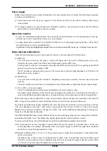
Power supply
Sudden noise-induced power supply fluctuations will cause malfunctions. Consider the following precautions
to avoid such malfunctions.
(1) Form connections from the power supply to LV
DD
, HV
DD
, and the V
SS
pin with the shortest, thickest pat-
terns possible.
(2) If a bypass capacitor is connected between LV
DD
/HV
DD
and V
SS
, the connection between the LV
DD
/HV
DD
pins and the V
SS
pin should be as short as possible.
Signal line location
• To prevent electromagnetically-induced noise caused by mutual inductance, avoid locating large-current sig-
nal lines near circuits susceptible to noise (e.g., clock inputs).
• Locating signal lines in parallel over significant distances or crossing high-speed signal lines will result in
mutual interference, noise, and malfunctions.
In particular, avoid positioning high-speed signal lines close to circuits susceptible to noise (e.g., clock input components).
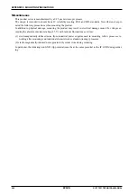
Noise-induced malfunctions
Check the following three points if you suspect the presence of noise-induced IC malfunctions.
(1) DSIO pin
Low-level noise to this pin will cause a switch to Debug mode. The switch to Debug mode can be con-
firmed by the clock output from DCLK and a High signal from the DST2 pin.
For the product version, we recommend connecting the DSIO pin directly to HV
DD
or pulling up the DISO
pin using a resistor not exceeding 10 k
Ω
.
The IC includes an internal pull-up resistor. The resistor has a relatively high impedance of 50 k
Ω
to 100
k
Ω
and is not noise-resistant.
(2) #RESET pin
Low-level noise to this pin will reset the IC. Depending on the input waveform, the reset may not proceed
correctly.
This is more likely to occur if, due to circuit design choices, the impedance is high when the reset input is High.
(3) LV
DD
, HV
DD
, V
SS
power supply
The IC will malfunction the instant noise falling below the rated voltage is input.
Incorporate countermeasures on the circuit board, including close patterns for circuit board power supply cir-
cuits, noise-filtering decoupling capacitors, and surge/noise prevention components on the power supply line.
Perform the inspections described above using an oscilloscope capable of observing waveforms of at least 200
MHz. It may not be possible to observe high-speed noise events with a low-speed oscilloscope.
If you detect potential noise-induced malfunctions while observing the waveform with an oscilloscope, recheck
with a low-impedance (less than 1 k
Ω
) resistor connecting the relevant pin to GND or to the power supply.
Malfunctions at that pin are likely if changes are visible, such as the malfunction disappearing, becoming less
frequent, or the phenomena changing.
The DSIO and #RESET input circuits described above detect input signal edges and are susceptible to malfunc-
tions induced by spike noise. This makes these digital signal pins the most susceptible to noise.
To reduce potential noise, keep the following two points in mind when designing circuit boards:
(A) It is important to use low impedance resistors when driving the signals, as described above. Avoid con-
necting impedance exceeding 1 k
Ω
(ideally, 0
Ω
) to the power supply or GND. The signal lines connected
should be no longer than approximately 5 mm.
(B) Signals switching from 1 to 0 or 0 to 1 may generate noise if signal lines run parallel to other digital lines
on the circuit board.
The highest risk of noise occurs in configurations in which a line is sandwiched between multiple signal
lines that vary in synchrony. You can minimize noise effects by reducing the length of parallel sections (limit
to a few cm) or by increasing the separation (to at least 2 mm).
Содержание S1C17001
Страница 1: ...Technical Manual S1C17001 CMOS 16 BIT SINGLE CHIP MICROCONTROLLER ...
Страница 31: ...3 MEMORY MAP AND BUS CONTROL 22 EPSON S1C17001 TECHNICAL MANUAL This page intentionally left blank ...
Страница 33: ...4 POWER SUPPLY VOLTAGE 24 EPSON S1C17001 TECHNICAL MANUAL This page intentionally left blank ...
Страница 63: ...6 INITERRUPT CONTROLLER 54 EPSON S1C17001 TECHNICAL MANUAL This page intentionally left blank ...
Страница 87: ...8 CLOCK GENERATOR CLG 78 EPSON S1C17001 TECHNICAL MANUAL This page intentionally left blank ...
Страница 91: ...9 PRESCALER PSC 82 EPSON S1C17001 TECHNICAL MANUAL This page intentionally left blank ...
Страница 133: ...11 16 BIT TIMER T16 124 EPSON S1C17001 TECHNICAL MANUAL This page intentionally left blank ...
Страница 185: ...14 8 BIT OSC1 TIMER T8OSC1 176 EPSON S1C17001 TECHNICAL MANUAL This page intentionally left blank ...
Страница 211: ...16 STOPWATCH TIMER SWT 202 EPSON S1C17001 TECHNICAL MANUAL This page intentionally left blank ...
Страница 219: ...17 WATCHDOG TIMER WDT 210 EPSON S1C17001 TECHNICAL MANUAL This page intentionally left blank ...
Страница 241: ...18 UART 232 EPSON S1C17001 TECHNICAL MANUAL This page intentionally left blank ...
Страница 277: ...20 I2 C 268 EPSON S1C17001 TECHNICAL MANUAL This page intentionally left blank ...
Страница 297: ...21 REMOTE CONTROLLER REMC 288 EPSON S1C17001 TECHNICAL MANUAL This page intentionally left blank ...
Страница 303: ...22 ON CHIP DEBUGGER DBG 294 EPSON S1C17001 TECHNICAL MANUAL This page intentionally left blank ...
Страница 313: ...25 PACKAGE 304 EPSON S1C17001 TECHNICAL MANUAL This page intentionally left blank ...


