10 INPUT/OUTPUT PORT (P)
96
EPSON
S1C17001 TECHNICAL MANUAL
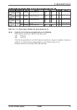
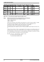
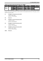
0x5203/0x5213/0x5223/0x5233: P
x
Port Pull-up Control Registers (P
x
_PU)
Register name Address
Bit
Name
Function
Setting
Init. R/W
Remarks
P0 Port Pull-up
Control Register
(P0_PU)
0x5203
(8 bits)
D7–0
P0PU[7:0]
P0[7:0] port pull-up enable
1 Enable
0 Disable
1
(0xff)
R/W
P1 Port Pull-up
Control Register
(P1_PU)
0x5213
(8 bits)
D7–0
P1PU[7:0]
P1[7:0] port pull-up enable
1 Enable
0 Disable
1
(0xff)
R/W
P2 Port Pull-up
Control Register
(P2_PU)
0x5223
(8 bits)
D7–0
P2PU[7:0]
P2[7:0] port pull-up enable
1 Enable
0 Disable
1
(0xff)
R/W
P3 Port Pull-up
Control Register
(P3_PU)
0x5233
(8 bits)
D7–4
–
reserved
–
–
–
0 when being read.
D3–0
P3PU[3:0]
P3[3:0] port pull-up enable
1 Enable
0 Disable
1
(0xff)
R/W
Note: The “
x
” in the bit names indicates the port number (0 to 3).
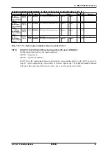
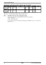
D[7:0] P
x
PU[7:0]: P
x
[7:0] Port Pull-up Enable Bits
(
P3 port is
P3PU[3:0])
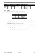
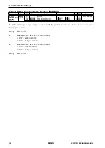
Enable or disable the pull-up resistor included in each port.
1 (R/W): Enabled (default)
0 (R/W): Disabled
P
x
PU[7:0] are the pull-up control bits that correspond directly to the P
x
[7:0] ports. Setting to 1 enables
the pull-up resistor and pulls up the port pin in input mode. It will not be pulled up if set to 0.
The
P
x
PU[7:0] setting is disabled in output mode, and the pin is not pulled up.
Input/output ports that are not used should be set with pull-up enabled.
This pull-up setting is also enabled for ports for which the peripheral module function has been select-
ed.
A delay will occur in the waveform rise-up depending on time constants such as pull-up resistance and
pin load capacitance if the port pin is switched from Low level to High level by the internal pull-up re-
sistor. An appropriate wait time must be set for the input/output port loading. The wait time set should
be a value not less than that calculated from the following equation.
Wait time = R
IN
x (C
IN
+ load capacitance on board) x 1.6 [s]
R
IN
: pull-up resistance maximum value
C
IN
: pin capacitance maximum value
Содержание S1C17001
Страница 1: ...Technical Manual S1C17001 CMOS 16 BIT SINGLE CHIP MICROCONTROLLER ...
Страница 31: ...3 MEMORY MAP AND BUS CONTROL 22 EPSON S1C17001 TECHNICAL MANUAL This page intentionally left blank ...
Страница 33: ...4 POWER SUPPLY VOLTAGE 24 EPSON S1C17001 TECHNICAL MANUAL This page intentionally left blank ...
Страница 63: ...6 INITERRUPT CONTROLLER 54 EPSON S1C17001 TECHNICAL MANUAL This page intentionally left blank ...
Страница 87: ...8 CLOCK GENERATOR CLG 78 EPSON S1C17001 TECHNICAL MANUAL This page intentionally left blank ...
Страница 91: ...9 PRESCALER PSC 82 EPSON S1C17001 TECHNICAL MANUAL This page intentionally left blank ...
Страница 133: ...11 16 BIT TIMER T16 124 EPSON S1C17001 TECHNICAL MANUAL This page intentionally left blank ...
Страница 185: ...14 8 BIT OSC1 TIMER T8OSC1 176 EPSON S1C17001 TECHNICAL MANUAL This page intentionally left blank ...
Страница 211: ...16 STOPWATCH TIMER SWT 202 EPSON S1C17001 TECHNICAL MANUAL This page intentionally left blank ...
Страница 219: ...17 WATCHDOG TIMER WDT 210 EPSON S1C17001 TECHNICAL MANUAL This page intentionally left blank ...
Страница 241: ...18 UART 232 EPSON S1C17001 TECHNICAL MANUAL This page intentionally left blank ...
Страница 277: ...20 I2 C 268 EPSON S1C17001 TECHNICAL MANUAL This page intentionally left blank ...
Страница 297: ...21 REMOTE CONTROLLER REMC 288 EPSON S1C17001 TECHNICAL MANUAL This page intentionally left blank ...
Страница 303: ...22 ON CHIP DEBUGGER DBG 294 EPSON S1C17001 TECHNICAL MANUAL This page intentionally left blank ...
Страница 313: ...25 PACKAGE 304 EPSON S1C17001 TECHNICAL MANUAL This page intentionally left blank ...

