3 MEMORY MAP AND BUS CONTROL
14
EPSON
S1C17001 TECHNICAL MANUAL
3.1 Bus Cycle
The CPU operates using CCLK as a datum. For more information on CCLK, refer to “8.2 CPU Core Clock (CCLK)
Control.”
The time from one CCLK rise-up to the next forms 1 CCLK, defined as one bus cycle. As shown in Figure 3.1, the
number of cycles required for a single bus access depends on the peripheral circuits and memory. The number of
bus accesses also varies and depends on the CPU command (access size) and device size.
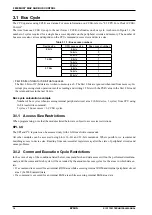
Table 3.1.1: Bus access numbers
Device size
CPU access size
Bus access number
8 bits
8 bits
1
16
bits
2
32
bits
*
4
16 bits
8 bits
1
16
bits
1
32
bits
*
2
32 bits
8 bits
1
16
bits
1
32
bits
*
1
∗
First 8 bits of data for 32-bit data access
The first 8 bits of 32-bit data are written to memory as 0. The first 8 bits are ignored when read from memory. In-
terrupt processing stack operation involves reading and writing 32 bits with the PSR value in the first 8 bits and
the return address in the last 24 bits.
Bus cycle calculation example
Number of bus cycles when accessing internal peripheral circuit area 2 (8-bit device, 3 cycles) from CPU using
16-bit read/write command:
3 cycles x 2 bus accesses = 6 CCLK cycles
3.1.1 Access Size Restrictions
When programming, note that the modules listed below are subject to access size restrictions.
SPI, I
2
C
The SPI and I
2
C registers can be accessed only with 16-bit read/write commands.
All other modules can be accessed using 8-bit, 16-bit, and 32-bit commands. Where possible, we recommend
matching access to device size. Reading from non-essential registers may alter the state of peripheral circuits and
cause problems.
3.1.2 Command Execution Cycle Restrictions
In the event of any of the conditions listed below, command fetch and data access will not be performed simultane-
ously, and the command fetch cycle will be extended by the amount of access cycles for the areas in which data ex-
ists.
• If a command is executed for an internal ROM area while accessing internal ROM and internal peripheral circuit
area 2 (0x5000 onward) data
• If a command is executed for an internal RAM area while accessing internal RAM area data
Содержание S1C17001
Страница 1: ...Technical Manual S1C17001 CMOS 16 BIT SINGLE CHIP MICROCONTROLLER ...
Страница 31: ...3 MEMORY MAP AND BUS CONTROL 22 EPSON S1C17001 TECHNICAL MANUAL This page intentionally left blank ...
Страница 33: ...4 POWER SUPPLY VOLTAGE 24 EPSON S1C17001 TECHNICAL MANUAL This page intentionally left blank ...
Страница 63: ...6 INITERRUPT CONTROLLER 54 EPSON S1C17001 TECHNICAL MANUAL This page intentionally left blank ...
Страница 87: ...8 CLOCK GENERATOR CLG 78 EPSON S1C17001 TECHNICAL MANUAL This page intentionally left blank ...
Страница 91: ...9 PRESCALER PSC 82 EPSON S1C17001 TECHNICAL MANUAL This page intentionally left blank ...
Страница 133: ...11 16 BIT TIMER T16 124 EPSON S1C17001 TECHNICAL MANUAL This page intentionally left blank ...
Страница 185: ...14 8 BIT OSC1 TIMER T8OSC1 176 EPSON S1C17001 TECHNICAL MANUAL This page intentionally left blank ...
Страница 211: ...16 STOPWATCH TIMER SWT 202 EPSON S1C17001 TECHNICAL MANUAL This page intentionally left blank ...
Страница 219: ...17 WATCHDOG TIMER WDT 210 EPSON S1C17001 TECHNICAL MANUAL This page intentionally left blank ...
Страница 241: ...18 UART 232 EPSON S1C17001 TECHNICAL MANUAL This page intentionally left blank ...
Страница 277: ...20 I2 C 268 EPSON S1C17001 TECHNICAL MANUAL This page intentionally left blank ...
Страница 297: ...21 REMOTE CONTROLLER REMC 288 EPSON S1C17001 TECHNICAL MANUAL This page intentionally left blank ...
Страница 303: ...22 ON CHIP DEBUGGER DBG 294 EPSON S1C17001 TECHNICAL MANUAL This page intentionally left blank ...
Страница 313: ...25 PACKAGE 304 EPSON S1C17001 TECHNICAL MANUAL This page intentionally left blank ...


