19 SPI
246
EPSON
S1C17001 TECHNICAL MANUAL
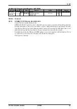
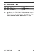
0x4326: SPI Control Register (SPI_CTL)
Register name Address
Bit
Name
Function
Setting
Init. R/W
Remarks
SPI Control
Register
(SPI_CTL)
0x4326
(16 bits)
D15–6
–
reserved
–
–
–
0 when being read.
D5
SPRIE
Receive data buffer full int. enable 1 Enable
0 Disable
0
R/W
D4
SPTIE
Transmit data buffer empty int.
enable
1 Enable
0 Disable
0
R/W
D3
CPHA
Clock phase select
1 Data out
0 Data in
0
R/W These bits must be
set before setting
SPEN to 1.
D2
CPOL
Clock polarity select
1 Active L
0 Active H
0
R/W
D1
MSSL
Master/slave mode select
1 Master
0 Slave
0
R/W
D0
SPEN
SPI enable
1 Enable
0 Disable
0
R/W
D[15:6] Reserved
D5
SPRIE: Receive Data Buffer Full Interrupt Enable Bit
D5
SPRIE: Receive Data Buffer Full Interrupt Enable Bit
Permits or prohibits receive data buffer full SPI interrupts.
1 (R/W): Permitted
0 (R/W): Prohibited (default)
Setting SPRIE to 1 permits the output of SPI interrupt requests to the ITC due to a receive data buffer
full. These interrupt requests are generated when the data received in the shift register is transferred to
the receive data buffer (when receipt is complete).
SPI interrupts are not generated by receive data buffer full if SPRIE is set to 0.
D4
SPTIE: Transmit Data Buffer Empty Interrupt Enable Bit
Permits or prohibits transmit data buffer empty SPI interrupts.
1 (R/W): Permitted
0 (R/W): Prohibited (default)
Setting SPTIE to 1 permits the output of SPI interrupt requests to the ITC due to a transmit data buffer
empty. These interrupt requests are generated when the data written to the transmit data buffer is trans-
ferred to the shift register (when transmission starts).
SPI interrupts are not generated by transmit data buffer empty if SPTIE is set to 0.
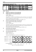
D3
CPHA: SPI Clock Phase Select Bit
Selects the SPI clock phase. (Default: 0)
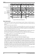
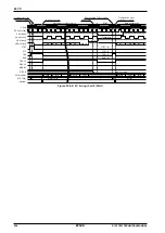
Sets the data transfer timing together with CPOL (D2). (See Figure 19.7.1.)
D2
CPOL: SPI Clock Polarity Select Bit
Selects the SPI clock polarity.
1 (R/W): Active Low
0 (R/W): Active High (default)
Sets the data transfer timing together with CPHA (D3). (See Figure 19.7.1.)
SPICLK(CPOL = 1, CPHA = 1)
SPICLK(CPOL = 1, CPHA = 0)
SPICLK(CPOL = 0, CPHA = 1)
SPICLK(CPOL = 0, CPHA = 0)
SDI/SDO
Receive data load timing
to shift register
D7 (MSB)
D0 (LSB)
Figure 19.7.1: Clock and data transfer timing
Содержание S1C17001
Страница 1: ...Technical Manual S1C17001 CMOS 16 BIT SINGLE CHIP MICROCONTROLLER ...
Страница 31: ...3 MEMORY MAP AND BUS CONTROL 22 EPSON S1C17001 TECHNICAL MANUAL This page intentionally left blank ...
Страница 33: ...4 POWER SUPPLY VOLTAGE 24 EPSON S1C17001 TECHNICAL MANUAL This page intentionally left blank ...
Страница 63: ...6 INITERRUPT CONTROLLER 54 EPSON S1C17001 TECHNICAL MANUAL This page intentionally left blank ...
Страница 87: ...8 CLOCK GENERATOR CLG 78 EPSON S1C17001 TECHNICAL MANUAL This page intentionally left blank ...
Страница 91: ...9 PRESCALER PSC 82 EPSON S1C17001 TECHNICAL MANUAL This page intentionally left blank ...
Страница 133: ...11 16 BIT TIMER T16 124 EPSON S1C17001 TECHNICAL MANUAL This page intentionally left blank ...
Страница 185: ...14 8 BIT OSC1 TIMER T8OSC1 176 EPSON S1C17001 TECHNICAL MANUAL This page intentionally left blank ...
Страница 211: ...16 STOPWATCH TIMER SWT 202 EPSON S1C17001 TECHNICAL MANUAL This page intentionally left blank ...
Страница 219: ...17 WATCHDOG TIMER WDT 210 EPSON S1C17001 TECHNICAL MANUAL This page intentionally left blank ...
Страница 241: ...18 UART 232 EPSON S1C17001 TECHNICAL MANUAL This page intentionally left blank ...
Страница 277: ...20 I2 C 268 EPSON S1C17001 TECHNICAL MANUAL This page intentionally left blank ...
Страница 297: ...21 REMOTE CONTROLLER REMC 288 EPSON S1C17001 TECHNICAL MANUAL This page intentionally left blank ...
Страница 303: ...22 ON CHIP DEBUGGER DBG 294 EPSON S1C17001 TECHNICAL MANUAL This page intentionally left blank ...
Страница 313: ...25 PACKAGE 304 EPSON S1C17001 TECHNICAL MANUAL This page intentionally left blank ...

