20 I
2
C
S1C17001 TECHNICAL MANUAL
EPSON
263
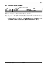
0x4342: I
2
C Control Register (I2C_CTL)
Register name Address
Bit
Name
Function
Setting
Init. R/W
Remarks
I
2
C Control
Register
(I2C_CTL)
0x4342
(16 bits)
D15–10
–
reserved
–
–
–
0 when being read.
D9
RBUSY
Receive busy flag
1 Busy
0 Idle
0
R
D8
TBUSY
Transmit busy flag
1 Busy
0 Idle
0
R
D7–5
–
reserved
–
–
–
0 when being read.
D4
NSERM
Noise remove on/off
1 On
0 Off
0
R/W
D3–2
–
reserved
–
–
–
0 when being read.
D1
STP
Stop control
1 Stop
0 Ignored
0
R/W
D0
STRT
Start control
1 Start
0 Ignored
0
R/W
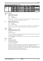
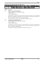
D[15:10] Reserved
D9
RBUSY: Receive Busy Flag
Indicates the I
2
C receipt status.
1 (R):
Operating
0 (R):
Standby (default)
RBUSY is set to 1 when the I
2
C starts data receiving and is maintained at 1 while receiving is under-
way. It is cleared to 0 once receipt is complete or in Wait state.
D8
TBUSY: Transmit Busy Flag
Indicates the I
2
C transmission status.
1 (R):
Operating
0 (R):
Standby (default)
TBUSY is set to 1 when the I
2
C starts data transmission and is maintained at 1 while transmission is
underway. It is cleared to 0 once transmission is complete. It is also returned to 0 in Wait state.
D[7:5] Reserved
D4
NSERM: Noise Remove On/Off Bit
Turns the noise filter function on or off.
1 (R/W): On
0 (R/W): Off (default)
The
I
2
C module incorporates a function for filtering noise from the SDA and SCL pin input signals.
This function is enabled by setting NSERM to 1.
Note that using this function requires setting the I
2
C clock (16-bit timer Ch.2 output clock) frequency to
1/6 or less of PCLK.
D[3:2] Reserved
D1
STP: Stop Control Bit
Generates the stop condition.
1 (R/W): Stop condition generated
0 (R/W): Disabled (default)
With STP set at 1, the I
2
C module generates the stop condition by changing the SDA line from Low to
High while maintaining the I
2
C bus SCL line at High. The I
2
C bus subsequently becomes free.
Note that the stop condition will be generated only if STP is 1 and TXE (D9/I2C_DAT register), RXE
(D10/I2C_DAT register), and STRT (D0) are set to 0 when data transfer is complete (including ACK
transfer). STP is disabled if any of TXE, RXE, or STRT is 1.
STP is automatically reset to 0 if the stop condition is generated.
Содержание S1C17001
Страница 1: ...Technical Manual S1C17001 CMOS 16 BIT SINGLE CHIP MICROCONTROLLER ...
Страница 31: ...3 MEMORY MAP AND BUS CONTROL 22 EPSON S1C17001 TECHNICAL MANUAL This page intentionally left blank ...
Страница 33: ...4 POWER SUPPLY VOLTAGE 24 EPSON S1C17001 TECHNICAL MANUAL This page intentionally left blank ...
Страница 63: ...6 INITERRUPT CONTROLLER 54 EPSON S1C17001 TECHNICAL MANUAL This page intentionally left blank ...
Страница 87: ...8 CLOCK GENERATOR CLG 78 EPSON S1C17001 TECHNICAL MANUAL This page intentionally left blank ...
Страница 91: ...9 PRESCALER PSC 82 EPSON S1C17001 TECHNICAL MANUAL This page intentionally left blank ...
Страница 133: ...11 16 BIT TIMER T16 124 EPSON S1C17001 TECHNICAL MANUAL This page intentionally left blank ...
Страница 185: ...14 8 BIT OSC1 TIMER T8OSC1 176 EPSON S1C17001 TECHNICAL MANUAL This page intentionally left blank ...
Страница 211: ...16 STOPWATCH TIMER SWT 202 EPSON S1C17001 TECHNICAL MANUAL This page intentionally left blank ...
Страница 219: ...17 WATCHDOG TIMER WDT 210 EPSON S1C17001 TECHNICAL MANUAL This page intentionally left blank ...
Страница 241: ...18 UART 232 EPSON S1C17001 TECHNICAL MANUAL This page intentionally left blank ...
Страница 277: ...20 I2 C 268 EPSON S1C17001 TECHNICAL MANUAL This page intentionally left blank ...
Страница 297: ...21 REMOTE CONTROLLER REMC 288 EPSON S1C17001 TECHNICAL MANUAL This page intentionally left blank ...
Страница 303: ...22 ON CHIP DEBUGGER DBG 294 EPSON S1C17001 TECHNICAL MANUAL This page intentionally left blank ...
Страница 313: ...25 PACKAGE 304 EPSON S1C17001 TECHNICAL MANUAL This page intentionally left blank ...


