10 INPUT/OUTPUT PORT (P)
88
EPSON
S1C17001 TECHNICAL MANUAL
10.6 P0 Port Chattering Filter Function
The P0 port includes a chattering filter circuit for key entry, which you can select to use or not use (and for which
you can select a verification time if used) individually for the four P0[3:0] and P0[7:4] ports using P0CF
x
[2:0]
(P0_CHAT register).
∗
P0CF1[2:0]
: P0[3:0] Chattering Filter Time Select Bits in the P0 Port Chattering Filter Control (P0_CHAT)
Register (D[2:0]/0x5208)
∗
P0CF2[2:0]
: P0[7:4] Chattering Filter Time Select Bits in the P0 Port Chattering Filter Control (P0_CHAT)
Register (D[6:4]/0x5208)
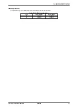
Table 10.6.1: Chattering filter function settings
P0CF
x
[2:0]
Verification time
*
0x7
16384/f
PCLK
(8ms)
0x6
8192/f
PCLK
(4ms)
0x5
4096/f
PCLK
(2ms)
0x4
2048/f
PCLK
(1ms)
0x3
1024/f
PCLK
(512μs)
0x2
512/f
PCLK
(256μs)
0x1
256/f
PCLK
(128μs)
0x0
No verification time
(Off)
(Default: 0x0,
*
when OSC3 = 2 MHz and PCLK = OSC3)
Note: • The chattering filter verification time refers to the maximum pulse width that can be filtered.
Generating an input interrupt requires a minimum input time of the verification time and a
maximum input time of twice the verification time.
• Input interrupts will not be accepted for a transition into SLEEP mode with the chattering
filter left on. The chattering filter should be set off (no verification time) before executing the
slp command.
• P0 port interrupts must be blocked when P0_CHAT register (0x5208) settings are being
changed. Changing the setting while interrupts are permitted may generate inadvertent P0
interrupts.
• A phenomenon may occur in which the internal signal oscillates due to the time elapsed
until the signal reaches the threshold value if the input signal rise-up/drop-off time is de-
layed. Since input interrupts will malfunction under these conditions, the input signal rise-
up/drop-off time should normally be set to 25 ns or less.
Содержание S1C17001
Страница 1: ...Technical Manual S1C17001 CMOS 16 BIT SINGLE CHIP MICROCONTROLLER ...
Страница 31: ...3 MEMORY MAP AND BUS CONTROL 22 EPSON S1C17001 TECHNICAL MANUAL This page intentionally left blank ...
Страница 33: ...4 POWER SUPPLY VOLTAGE 24 EPSON S1C17001 TECHNICAL MANUAL This page intentionally left blank ...
Страница 63: ...6 INITERRUPT CONTROLLER 54 EPSON S1C17001 TECHNICAL MANUAL This page intentionally left blank ...
Страница 87: ...8 CLOCK GENERATOR CLG 78 EPSON S1C17001 TECHNICAL MANUAL This page intentionally left blank ...
Страница 91: ...9 PRESCALER PSC 82 EPSON S1C17001 TECHNICAL MANUAL This page intentionally left blank ...
Страница 133: ...11 16 BIT TIMER T16 124 EPSON S1C17001 TECHNICAL MANUAL This page intentionally left blank ...
Страница 185: ...14 8 BIT OSC1 TIMER T8OSC1 176 EPSON S1C17001 TECHNICAL MANUAL This page intentionally left blank ...
Страница 211: ...16 STOPWATCH TIMER SWT 202 EPSON S1C17001 TECHNICAL MANUAL This page intentionally left blank ...
Страница 219: ...17 WATCHDOG TIMER WDT 210 EPSON S1C17001 TECHNICAL MANUAL This page intentionally left blank ...
Страница 241: ...18 UART 232 EPSON S1C17001 TECHNICAL MANUAL This page intentionally left blank ...
Страница 277: ...20 I2 C 268 EPSON S1C17001 TECHNICAL MANUAL This page intentionally left blank ...
Страница 297: ...21 REMOTE CONTROLLER REMC 288 EPSON S1C17001 TECHNICAL MANUAL This page intentionally left blank ...
Страница 303: ...22 ON CHIP DEBUGGER DBG 294 EPSON S1C17001 TECHNICAL MANUAL This page intentionally left blank ...
Страница 313: ...25 PACKAGE 304 EPSON S1C17001 TECHNICAL MANUAL This page intentionally left blank ...

