APPENDIX C MOUNTING PRECAUTIONS
332
EPSON
S1C17001 TECHNICAL MANUAL
Appendix C: Mounting Precautions
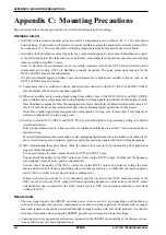
This section describes various precautions for circuit board design and IC mounting.
Oscillator circuit
• Oscillation characteristics depend on factors such as components used (oscillator, R
f
, C
G
, C
D
) and circuit
board patterns. In particular, with ceramic or crystal oscillators, select the appropriate external resistors (R
f
,)
and capacitors (C
G
, C
D
) only after fully evaluating components actually mounted on the circuit board.
• Oscillator clock disturbances caused by noise may cause malfunctions. To prevent such disturbances, consid-
er the following points. The latest devices, in particular, are manufactured by microscopic processes, making
them especially susceptible to noise.
Areas in which noise countermeasures are especially important include the OSC2 pin and related circuit
components and wiring. OSC1 pin handling is equally important. The noise precautions required for the
OSC1 and OSC2 pins are described below.
We also recommend applying similar noise countermeasures to high-speed oscillator circuits, such as the
OSC3 and OSC4 pins and wiring.
(1) Components such as oscillators, resistors, and capacitors connected to the OSC1 (OSC3) and OSC2 (OSC4)
pins should have the shortest connections possible.
(2) Wherever possible, avoid locating digital signal lines within 3 mm of the OSC1 (OSC3) and OSC2 (OSC4)
pins or related circuit components and wiring. Rapidly-switching signals, in particular, should be kept at a dis-
tance from these components. Since the spacing between layers of multi-layer printed circuit boards is a mere 0.1
mm to 0.2 mm, the above precautions also apply when positioning digital signal lines on other layers.
Never place digital signal lines alongside such components or wiring, even if more than 3 mm distance or
located on other layers. Avoid crossing wires.
(3) Use V
SS
to shield OSC1 (OSC3) and OSC2 (OSC4) pins and related wiring (including wiring for adjacent
circuit board layers).
Fully ground adjacent layers, where possible. At minimum, shield the area at least 5 mm around the above
pins and wiring.
Even after implementing these precautions, avoid configuring digital signal lines in parallel, as described in (2)
above. Avoid crossing even on discrete layers, except for lines carrying signals with low switching frequencies.
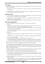
(4) After implementing these precautions, check the output clock waveform by running the actual application
program within the product.
Use an oscilloscope to check outputs from the FOUT1 and FOUT3 pins.
You can check the quality of the OSC3 output waveform via the FOUT3 output. Confirm that the frequency
is as designed, is free of noise, and has minimal jitter.
You can check the quality of the OSC1 waveform via the FOUT1 output. In particular, enlarge the areas
before and after the clock rising and falling edges and take special care to confirm that the regions approxi-
mately 100 ns to either side are free of clock or spiking noise.
Failure to observe precautions (1) to (3) adequately may lead to jitter in the OSC3 output and noise in the
OSC1 output. Jitter in the OSC3 output will reduce operating frequencies, while noise in the OSC1 output
will destabilize timers operated by the OSC1 clock as well as CPU core operations when the system clock
switches to OSC1.
Reset circuit
• The reset signal input to the #RESET pin when power is turned on will vary, depending on various factors,
such as power supply start-up time, components used, and circuit board patterns. Constants such as capaci-
tance and resistance should be determined through thorough testing with real-world products. Account for
resistance fluctuations when setting the #RESET pin pull-up resistance for constants settings.
• Components such as capacitors and resistors connected to the #RESET pin should have the shortest connec-
tions possible to prevent noise-induced resets.
Содержание S1C17001
Страница 1: ...Technical Manual S1C17001 CMOS 16 BIT SINGLE CHIP MICROCONTROLLER ...
Страница 31: ...3 MEMORY MAP AND BUS CONTROL 22 EPSON S1C17001 TECHNICAL MANUAL This page intentionally left blank ...
Страница 33: ...4 POWER SUPPLY VOLTAGE 24 EPSON S1C17001 TECHNICAL MANUAL This page intentionally left blank ...
Страница 63: ...6 INITERRUPT CONTROLLER 54 EPSON S1C17001 TECHNICAL MANUAL This page intentionally left blank ...
Страница 87: ...8 CLOCK GENERATOR CLG 78 EPSON S1C17001 TECHNICAL MANUAL This page intentionally left blank ...
Страница 91: ...9 PRESCALER PSC 82 EPSON S1C17001 TECHNICAL MANUAL This page intentionally left blank ...
Страница 133: ...11 16 BIT TIMER T16 124 EPSON S1C17001 TECHNICAL MANUAL This page intentionally left blank ...
Страница 185: ...14 8 BIT OSC1 TIMER T8OSC1 176 EPSON S1C17001 TECHNICAL MANUAL This page intentionally left blank ...
Страница 211: ...16 STOPWATCH TIMER SWT 202 EPSON S1C17001 TECHNICAL MANUAL This page intentionally left blank ...
Страница 219: ...17 WATCHDOG TIMER WDT 210 EPSON S1C17001 TECHNICAL MANUAL This page intentionally left blank ...
Страница 241: ...18 UART 232 EPSON S1C17001 TECHNICAL MANUAL This page intentionally left blank ...
Страница 277: ...20 I2 C 268 EPSON S1C17001 TECHNICAL MANUAL This page intentionally left blank ...
Страница 297: ...21 REMOTE CONTROLLER REMC 288 EPSON S1C17001 TECHNICAL MANUAL This page intentionally left blank ...
Страница 303: ...22 ON CHIP DEBUGGER DBG 294 EPSON S1C17001 TECHNICAL MANUAL This page intentionally left blank ...
Страница 313: ...25 PACKAGE 304 EPSON S1C17001 TECHNICAL MANUAL This page intentionally left blank ...

