282
c
HELP Mode Function and Operation Procedures
chap.7
2
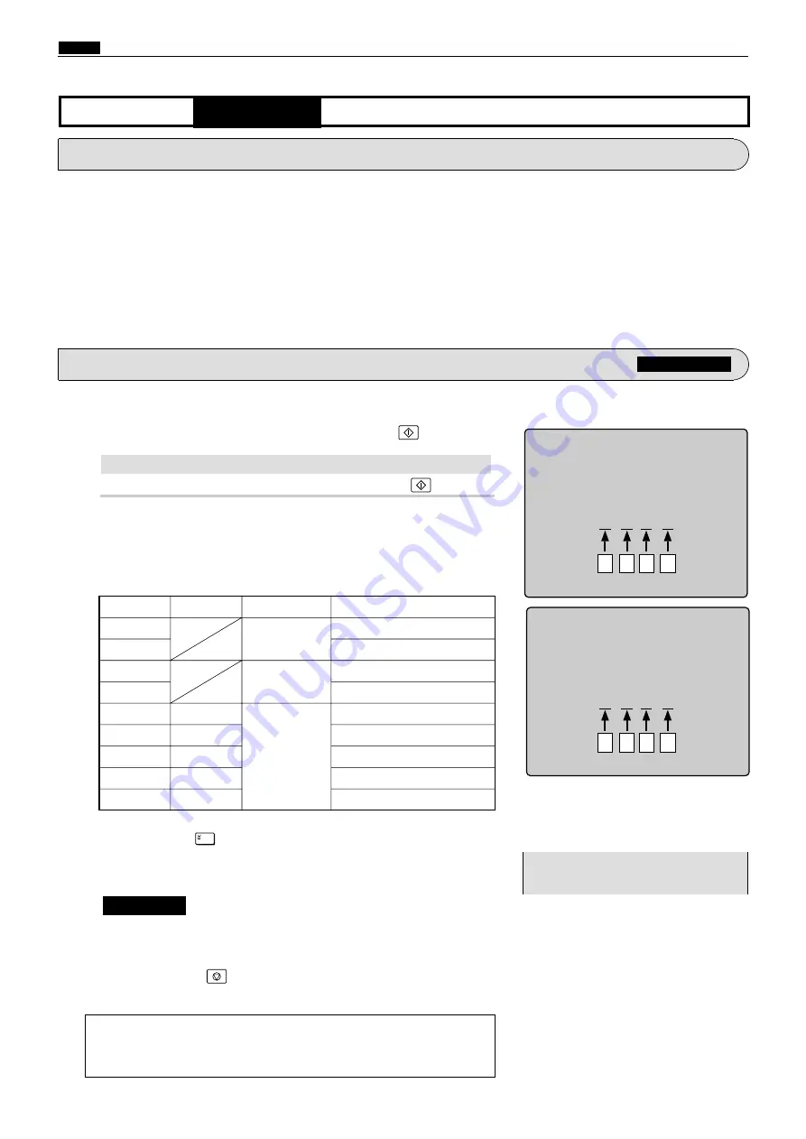
Access HELP mode
H-57
, and press the
key.
1 line scan time (H-57)
H-52, H-57
(1) Adjustment / specification setting
HELP mode
H-52
00**
11**
**0*
**1*
***1
***0
***1
***0
H-57
0***
0***
1***
1***
Item
I / F auto / manual
setting
DP-10
test pattern
Setting
Manual
Auto(standard)
Standard
DP-10 test pattern only
1.6m sec / line
2.0m sec / line(standard)
3.2m sec / line
4.0m sec / line
0000
0000
Factory setting
1 line process /
scan time
e
Press the [
=
] key.
The correction amount will be memorized in the battery PCB unit's
EEPROM. During memorization,
"SAVE"
will be displayed.
Do not turn off the power before the "SAVE" display has disappeared.
1. Functions
(1) I/ F switch,DP-10 test pattern,1 line process time setting
¡
Following items are indicated.
A : I/F switch(H-52)
B : DP-10 test pattern(H-52)
C,D : 1 line process time(H-52), 1 line scan time(H-57)
(1)I/ F switch,DP-10 test pattern,1 line process time setting
¡
During memorization:
IMPORTANT :
2. Operation procedure
Accessing HELP modes
a
See page 219
q
Access HELP mode
H-52
, and press the
key.
HELP-052
Adjustment/Specification setting
1111
w
Use the [
0
] and [
1
] numeric keys to enter a 4-place binary
value for the desired correction amount.
See the table below for 4-place binary values and the corresponding
correction amounts.
a
To exit the HELP mode :
Turn the power switch OFF.
a
To access another HELP mode :
Enter the desired mode number
using the numeric keys.
r
Press the
STOP
key.
The HELP mode selection display will reappear.
A
B
C
D
- SAVE -
HELP-057
Adjustment/Specification setting
1111
A
B
C
D
Содержание Duprinter DP-330
Страница 9: ......
Страница 11: ......
Страница 18: ...c Dimensions chap 1 17 MEMO...
Страница 24: ...4 8 2A 2B 2C 44000A1e b Part Names and Their Functions chap 1 23...
Страница 152: ...151 MEMO...
Страница 193: ...192 MEMO...
Страница 328: ...327 x Overall Wiring Layout chap 8 14 2 Overall Wiring Layout 2 Overall Wiring Layout 2 Drive PCB 1 2 O...
Страница 329: ...328 x Overall Wiring Layout chap 8 15 Overall Wiring Layout 2 Drive PCB 2 2...


