208
z
Troubleshooting Guide
chap.6
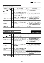
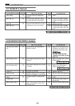
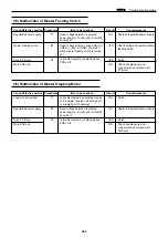
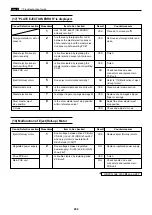
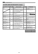
(25) "PAPER JAM ON THE EJECTION SIDE" is displayed
Cause/Defective section Procedures
Item to be checked
Result
Countermeasure
Paper
1
NO
Use paper conforming to
specification.
2
YES
Proceed to procedure
7
.
Paper jammed
3
YES
Refer to “(29) Paper JAM in
paper eject side”.
Master ejection box is
4
YES
Finish.
not closed.
Dirt or foreign material
5
YES
Clean the photo-emitting and
on sensor
photo-receiving sections of JAM
sensor.
Sensor position
6
YES
Finish.
JAM sensor
7
YES
Replace JAM sensor photo-
photo-emitting PCB
emitting PCB.
JAM sensor
NO
Replace JAM sensor photo-
photo-receiving PCB
receiving PCB.
Drum stop/JAM detect
8
NO
Adjust position of the drum stop/JAM
position sensor
detect position sensor. If
necessary, replace.
Main PCB unit
YES
Replace main PCB unit.
Is printing paper long within specified
value?
When JAM sensor 1 is checked with
HELP mode (H-06)
*
, is 0 displayed if
sensor is photopassing and is 1 dis-
played if photointerrupted?
Is paper really jammed at master ejec-
tion section?
Is trouble cleared by properly closing
the master ejection box?
Is there any dirt or foreign material on
the JAM sensor photo-emitting or
photo-receiving section?
Is trouble cleared by adjusting the
JAM detection sensor position?
Is 0 displayed by directing another
light to the photo-receiving section of
the document sensor photo-receiving
PCB when JAM sensor 1 is checked
with HELP mode (H-06)
*
?
When drum is checked with HELP
mode (H-05)
*
while rotating slowly,
does the drum stop/JAM detect posi-
tion sensor display 0 or 1 according to
edge of photointerrupter?
\
see page 211
HELP mode H-05
\
see p.230
*
HELP mode H-06
\
see p.232
*
Содержание Duprinter DP-330
Страница 9: ......
Страница 11: ......
Страница 18: ...c Dimensions chap 1 17 MEMO...
Страница 24: ...4 8 2A 2B 2C 44000A1e b Part Names and Their Functions chap 1 23...
Страница 152: ...151 MEMO...
Страница 193: ...192 MEMO...
Страница 328: ...327 x Overall Wiring Layout chap 8 14 2 Overall Wiring Layout 2 Overall Wiring Layout 2 Drive PCB 1 2 O...
Страница 329: ...328 x Overall Wiring Layout chap 8 15 Overall Wiring Layout 2 Drive PCB 2 2...


