15. USI
A96G140/A96G148/A96A148 User’s manual
184
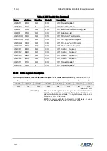
USInSCLR (USInSCL Low Period Register: For I2C mode): E6H/F6H, n = 0, 1
7
6
5
4
3
2
1
0
USInSCLR7
USInSCLR6
USInSCLR5
USInSCLR 4
USInSCLR 3
USInSCLR 2
USInSCLR 1
USInSCLR 0
R/W
R/W
R/W
R/W
R/W
R/W
R/W
R/W
Initial value: 3FH
USInSCLR[7:0]
This register defines the high period of SCLn when it operates in
I2C master mode.
The base clock is SCLK, the system clock, and the period is
calculated by the formula: t
SCLK
X (4 X US2) where
t
SCLK
is the period of SCLK.
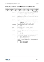
USInSAR (USIn Slave Address Register: For I2C mode): DDH/EDH, n = 0, 1
7
6
5
4
3
2
1
0
USInSLA6
USInSLA5
USInSLA4
USInSLA3
USInSLA2
USInSLA1
USInSLA0
USInGCE
R/W
R/W
R/W
R/W
R/W
R/W
R/W
R/W
Initial value: 00H
USInSLA[6:0]
These bits configure the slave address of I2C when it operates in
I2C slave mode.
USInGCE
This bit decides whether I2C allows general call address or not in
I2C slave mode.
0
Ignore general call address
1
Allow general call address


