5. Memory organization
A96G140/A96G148/A96A148 User’s manual
40
5.4.2
SFR map
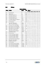
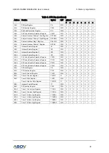
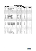
Table 5. SFR Map
Address Function
Symbol
R/W
@Reset
7
6
5
4
3
2
1
0
80H
P0 Data Register
P0
R/W
0
0
0
0
0
0
0
0
81H
Stack Pointer
SP
R/W
0
0
0
0
0
1
1
1
82H
Data Pointer Register Low
DPL
R/W
0
0
0
0
0
0
0
0
83H
Data Pointer Register High
DPH
R/W
0
0
0
0
0
0
0
0
84H
Data Pointer Register Low 1
DPL1
R/W
0
0
0
0
0
0
0
0
85H
Data Pointer Register High 1
DPH1
R/W
0
0
0
0
0
0
0
0
86H
Low Voltage Indicator Control Register
LVICR
R/W
–
–
0
0
0
0
0
0
87H
Power Control Register
PCON
R/W
0
–
–
–
0
0
0
0
88H
P1 Data Register
P1
R/W
0
0
0
0
0
0
0
0
89H
Watch Timer Data Register
WTDR
W
0
1
1
1
1
1
1
1
Watch Timer Counter Register
WTCNT
R
–
0
0
0
0
0
0
0
8AH
System and Clock Control Register
SCCR
R/W
–
–
–
–
–
–
0
0
8BH
Basic Interval Timer Control Register
BITCR
R/W
0
1
0
0
0
1
0
1
8CH
Basic Interval Timer Counter Register
BITCNT
R
0
0
0
0
0
0
0
0
8DH
Watch Dog Timer Control Register
WDTCR
R/W
0
0
0
–
–
–
0
0
8EH
Watch Dog Timer Data Register
WDTDR
W
1
1
1
1
1
1
1
1
Watch Dog Timer Counter Register
WDTCNT
R
0
0
0
0
0
0
0
0
8FH
BUZZER Data Register
BUZDR
R/W
1
1
1
1
1
1
1
1
90H
P2 Data Register
P2
R/W
0
0
0
0
0
0
0
0
91H
P0 Open-drain Selection Register
P0OD
R/W
0
0
0
0
0
0
0
0
92H
P1 Open-drain Selection Register
P1OD
R/W
0
0
0
0
0
0
0
0
93H
P2 Open-drain Selection Register
P2OD
R/W
0
0
0
0
0
0
0
0
94H
P4 Open-drain Selection Register
P4OD
R/W
0
0
0
0
0
0
0
0
95H
P5 Pull-up Resistor Selection Register
P5PU
R/W
–
–
0
0
0
0
0
0
96H
Watch Timer Control Register
WTCR
R/W
0
–
–
0
0
0
0
0
97H
BUZZER Control Register
BUZCR
R/W
–
–
–
–
–
0
0
0
98H
P3 Data Register
P3
R/W
0
0
0
0
0
0
0
0
9CH
A/D Converter Control Low Register
ADCCRL
R/W
0
0
0
0
0
0
0
0
9DH
A/D Converter Control High Register
ADCCRH
R/W
0
0
0
0
0
0
0
1
9EH
A/D Converter Data Low Register
ADCDRL
R
x
x
x
x
x
x
x
x
9FH
A/D Converter Data High Register
ADCDRH
R
x
x
x
x
x
x
x
x


