A96G140/A96G148/A96A148 User’s manual
18. Reset
225
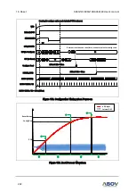
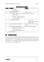
Table 42. Boot Process Description
Process
Description
Remarks
①
No Operation
LSIRC (128KHz) ON
0.7V to 0.9V
②
1st POR level Detection
About 1.1V to 1.3V
③
(LSIRC 128KHz/32)x32h Delay
section (=10ms)
VDD input voltage must rise over
than flash operating voltage for
Configure option read
Slew Rate
>=
0.025V/ms
④
Configure option read point
About 1.6V to 1.8V
Configure Value is determined
by Writing Option
⑤
Rising section to Reset Release Level
16ms point after POR or Ext_reset
release
⑥
Reset Release section (BIT overflow)
I.
after16ms, after External Reset
Release (External reset)
II.
16ms point after POR (POR only)
BIT is used for Peripheral stability
⑦
Normal operation
18.3
External resetb input
External resetb is input to a Schmitt trigger. If the resetb pin is held with low for at least 10us over within
the operating voltage range and stable oscillation, it is applied and the internal state is initialized. After
reset state becomes ‘1’, it needs stabilization time with 16ms and after
the stable state, the internal
reset
becomes ‘1’. The
reset process step needs 5 oscillator clocks. And the program execution starts
at the vector address stored at address 0000H.

