15. USI
A96G140/A96G148/A96A148 User’s manual
168
Note that during SPI mode of operation, the pin RXDn is renamed as MISOn and TXDn is renamed as
MOSIn for compatibility to other SPI devices.
15.11
USIn SPI clock formats and timing
To accommodate a wide variety of synchronous serial peripherals from different manufacturers, the
USIn has a clock polarity bit (CPOLn) and a clock phase control bit (CPHAn) to select one of four clock
formats for data transfers. CPOLn selectively insert an inverter in series with the clock. CPHAn chooses
between two different clock phase relationships between the clock and data. Note that CPHAn and
CPOLn bits in USInCR1 register have different meanings according to the USInMS[1:0] bits which
decides the operating mode of USIn.
Table 29 shows four combinations of CPOLn and CPHAn for SPI mode 0, 1, 2, and 3.
Table 30. CPOLn Functionality
SPI Mode
CPOLn
CPHAn
Leading Edge
Trailing Edge
0
0
0
Sample (Rising)
Setup (Falling)
1
0
1
Setup (Rising)
Sample (Falling)
2
1
0
Sample (Falling)
Setup (Rising)
3
1
1
Setup (Falling)
Sample (Rising)
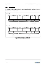
Figure 91. USIn SPI Clock Formats when CPHAn = 0
When CPHAn = 0, the slave begins to drive its MISOn output with the first data bit value when SSn
SCKn
(CPOLn=1)
MISOn
MOSIn
SCKn
(CPOLn=0)
/SSn OUT
(MASTER)
BIT7
BIT0
/SSn IN
(SLAVE)
BIT6
BIT1
…
…
BIT2
BIT5
BIT0
BIT7
BIT1
BIT6
SAMPLE
MSB First
LSB First


