A96G140/A96G148/A96A148 User’s manual
12. Timer 0/1/2/3/4/5
145
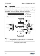
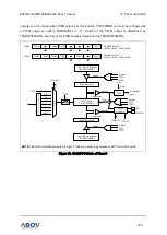
outputs up to 16-bit resolution PWM output. For this function, T5O/PWM5O pin must be configured as
a PWM output by setting P0FSRH[5:4
] to ‘
1
1’. Period of
the PWM output is determined by
T5ADRH/T5ADRL, and duty of the PWM output is determined by T5BDRH/T5BDRL.
T5MS[1:0]
T5POL
Reload
A Match
T5CC
T5EN
P
r
e
s
c
a
l
e
r
fx
M
U
X
fx/2
fx/4
fx/32
fx/128
fx/512
fx/8
fx/1
Comparator
16-bit Cou nte r
T5CNTH/T5CNTL
16-bit B Data Re gister
T5BDRH/T5BDRL
Clear
B Match
HIRC
Buffer Reg ister B
Comparator
16-bit A Data Re gister
T5ADRH/T5ADRL
T5IFR
S/W
Clear
To i nte rrupt
block
A Match
Buffer Reg ister A
Reload
Pulse
Gen erator
T5O
R
T5EN
3
T5CK[2:0]
2
A Match
T5CC
T5EN
A Match
T5CC
T5EN
T5EN
T5CRH
1
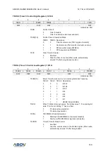
ADDRES S:1010H
INITIAL VALUE : 0000_0000B
–
T5MS1
T5MS0
–
–
–
T5CC
–
1
1
–
–
–
X
T5CK2
T5CRL
X
ADDRES S:1011H
INITIAL VALUE : 0000_0000B
T5CK1
T5CK0
T5IFR
–
T5POL
–
T5CNTR
X
X
X
–
X
–
X
PWM5O
NOTE
: T5EN is automatically cleared to logic
“0” after one pulse is generated at a PPG one-shot mode.
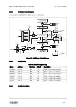
Figure 75. 16-bit PPG Mode of Timer 5


