A96G140/A96G148/A96A148 User’s manual
20 Development tools
257
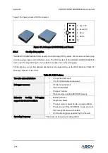
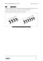
Figure 134 shows the standard 10-pin connector of the OCD 1 and OCD 2.
OCD 1
OCD 2
Figure 134. OCD 1 and OCD 2 Connector Pin Diagram
Table 56 describes the pins assigned to the OCD 1 and OCD 2.
Table 56. OCD 1 and OCD 2 Pin Description
Pin name
Microcontroller function in Debug Mode
I/O
Description
DSCL
I
Serial clock pin. Input only pin.
DSDA
I/O
Serial data pin.
Output port when reading and input port when programming.
It can be assigned as input/push-pull output port.
VDD,VSS
―
Logic power supply pin.
The OCD emulator supports
ABOV’s 8051 series MCU emulation. The OCD
uses two wires that are
interfaces between PC and MCU, which is attach
ed to user’s system. The OCD
can read or change the
value of MCU’s internal memory and I/O peri
pherals. In addition, the OCD
controls MCU’s internal
debugging logic. This means that the OCD controls emulation, step run, monitoring and many more
functions regarding debugging.
The OCD debugger program runs underneath MS operating system such as MS-Windows NT/ 2000/
XP/ Vista (32-bit).
If you want to see more details, please visit ABOV’s website (
),
and download debugger S/W and OCD debugger manuals.
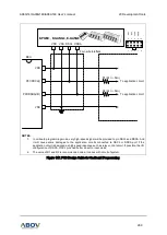
Connection:
—
DSCL (A96G140/A96G148/A96A148 P01 port)
—
DSDA (A96G140/A96G148/A96A148 P00 port)


