19. Memory programming
A96G140/A96G148/A96A148 User’s manual
236
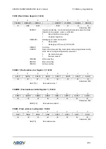
FEARM (Flash address middle Register): 1029H
7
6
5
4
3
2
1
0
ARM7
ARM6
ARM5
ARM4
ARM3
ARM2
ARM1
ARM0
W
W
W
W
W
W
W
W
Initial value: 00H
ARM[7:0]
Flash address middle
FEARH (Flash address high Register): 1028H
7
6
5
4
3
2
1
0
ARH7
ARH6
ARH5
ARH4
ARH3
ARH2
ARH1
ARH0
W
W
W
W
W
W
W
W
Initial value: 00H
ARH[7:0]
Flash address high
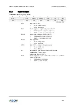
NOTES
:
1.
FEAR registers are used for program, erase and auto-verify. In program and erase mode, it is page
address and ignored the same least significant bits as the number of bits of page address. In auto-
verify mode, address increases automatically by one.
2.
EARs are write-only register. Reading these registers returns 24-bit checksum result.
3.
When calculating flash checksum, the lower 4 bits of start address are calculated as 0x0000 and the
lower 4 bits of end address as 0x1111 for protection.
4.
This device can support internal Checksum calculation, device verification time will be decreased
dramatically.
5.
Checksum cannot detect error address or error bit, but it is quite good feature in mass product
programming.
6.
Device data read out time takes few seconds. The execution time per byte is 4~5ms based on 16MHz.

