12. Timer 0/1/2/3/4/5
A96G140/A96G148/A96A148 User’s manual
94
12
Timer 0/1/2/3/4/5
12.1
Timer 0
An 8-bit timer 0 consists of a multiplexer, a timer 0 counter register, a timer 0 data register, a timer 0
capture data register and a timer 0 control register (T0CNT, T0DR, T0CDR, T0CR).
Timer 0 operates in one of three modes introduced in the followings:
8-bit timer/counter mode
8-bit PWM output mode
8-bit capture mode
Timer/counter 0 can be clocked by an internal or an external clock source (EC0). The clock source is
selected by clock selection logic which is controlled by clock selection bits T0CK[2:0].
TIMER0 clock source: f
X
/2, 4, 8, 32, 128, 512, 2048 and EC0
In capture mode, data is captured into input capture data register (T0CDR) by EINT10. In timer/counter
mode, whenever counter value is equal to T0DR, T0O port toggles. In addition, timer 0 outputs PWM
waveform through PWM0O port in the PWM mode.
Table 14. Timer 0 Operating Mode
T0EN
T0MS[1:0]
T0CK[2:0]
Timer 0
1
00
XXX
8-bit Timer/Counter Mode
1
01
XXX
8-bit PWM Mode
1
1X
XXX
8-bit Capture Mode
12.1.1
8-bit timer/counter mode
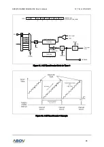
As shown in figure 29, 8-bit timer/counter mode is selected by control register.
8-bit timer has counter and data registers. The counter register is increased by internal or external clock
input. Timer 0 can use the input clock with one of 2, 4, 8, 32, 128, 512 and 2048 prescaler division rates
(T0CK[2:0]). When both values of T0CNT and T0DR are identical to each other in timer 0, a match
signal is generated and the interrupt of Timer 0 occurs.T0CNT value is automatically cleared by the
match signal, and can be cleared by software (T0CC) too.
External clock (EC0) counts up the timer at the rising edge. If the EC0 is selected as a clock source by
T0CK[2:0], EC0 port should be set as an input port by configuring P52IO bit.


