background image

V04.00 | 2021/05

227

14.4

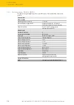
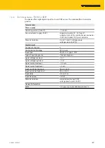
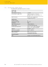
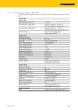
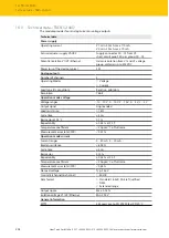
Technical data – TBEN-S2-8DIP

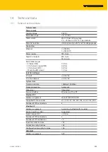
The device offers eight digital inputs for 3-wire PNP sensors. The module offers channel dia-
gnostics

Technical data

Power supply

Operating current (from V1)

< 150 mA

Sensor/actuator supply VAUX1

Supply connector C0…C3 from V1, 
supply at pin1 of the switchable per connector,
short-circuit proof, 0.5 A per connector

Potential isolation

From V1 and V2 voltage group,
voltages up to 500 VDC

Digital inputs

Number of channels

8

Connection technology

M12, 5-pin

Input type

EN 61131-2 type 3, PNP

Type of input diagnostics

Channel diagnosis

Signal voltage low level

< 5 V

Signal voltage high level

> 11 V

Signal current low level

< 1.5 mA

Signal current high level

> 2 mA

Input resistance low level

Min. 3,33 kΩ

Input resistance high level

Max. 5,5 kΩ

Input delay

0.2 ms/3 ms

Input frequency

400 Hz

Potential isolation

Galvanic isolation to P1/P2, 
voltage proof up to 500 VDC

General information

MTTF

314 years acc. to SN 29500 (Ed. 99) 20 °C

Summary of Contents for TBEN-S Series

Page 1: ...Your Global Automation Partner Instructions for Use TBEN S Digital and Analog Modules ...

Page 2: ...2 Hans Turck GmbH Co KG T 49 208 4952 0 F 49 208 4952 264 more turck com www turck com ...

Page 3: ...4 4 Possible Ethernet network structures 15 4 4 1 Ethernet daisy chain max number of connected modules 17 4 5 Technical accessories 18 5 Mounting 19 5 1 Mounting the device in Zone 2 and Zone 22 19 5 2 Combine TBEN S modules for mounting 19 5 2 1 Combine TBEN S modules for composite mounting to a mounting plate 19 5 2 2 Combine TBEN S modules for single and composite mounting on a DIN rail 20 5 3 ...

Page 4: ... PLC in PROFINET 64 8 5 1 Installing the GSDML file 64 8 5 2 Connecting the devices to the PLC 66 8 5 3 Configuring device functions 67 8 5 4 Assigning the PROFINET device name 68 8 5 5 Setting the IP address in TIA Portal 69 8 5 6 Setting module parameters 70 8 5 7 Going online with the PLC 71 8 5 8 PROFINET Mapping 71 8 6 Configuring devices at Modbus TCP 72 8 6 1 Implemented Modbus functions 72...

Page 5: ...ment value representation TBEN S2 4AO 204 10 Troubleshooting 217 11 Maintenance 218 11 1 Executing the firmware update 218 12 Repair 222 12 1 Returning devices 222 13 Disposal 222 14 Technical Data 223 14 1 General technical data 223 14 2 Techincal data TBEN S1 8DIP 225 14 3 Technical data TBEN S1 8DIP D 226 14 4 Technical data TBEN S2 8DIP 227 14 5 Technical data TBEN S1 8DOP 228 14 6 Technical d...

Page 6: ...Table of Contents 6 Hans Turck GmbH Co KG T 49 208 4952 0 F 49 208 4952 264 more turck com www turck com ...

Page 7: ...s situation with medium risk of death or severe in jury if not avoided CAUTION CAUTION indicates a dangerous situation of medium risk which may result in minor or moderate injury if not avoided NOTICE NOTICE indicates a situation which may lead to property damage if not avoided NOTE NOTE indicates tips recommendations and useful information on specific actions and facts The notes simplify your wor...

Page 8: ...N S2 4AI V 3 1 2 0 TBEN S2 4AO V 3 1 2 0 2 2 Scope of delivery The scope of delivery includes n Compact I O module n M8 or respectively M12 dummy plugs for connectors n Label clips 2 3 Legal requirements The device falls under the following EU directives n 2014 30 EU electromagnetic compatibility n 2011 65 EU RoHS Directive n 2014 34 EU ATEX Directive 2 4 Turck service Turck supports you with your...

Page 9: ...e assembled installed operated parameterized and maintained by professionally trained personnel n The device may only be used in accordance with applicable national and international regu lations standards and laws n The device only meets the EMC requirements for industrial areas and is not suitable for use in residential areas n Change the default password of the integrated web server after the f...

Page 10: ... analog devices provide four analog in or output channels The connectors for the digital I Os are designed as M8 or M12 sockets the connectors for the analog I Os as M12 sockets For the connection to Ethernet the devices provide two M8 sockets The power supply connectors are designed as 4 pin M8 connectors 4 1 Device overview mm Inch 132 5 20 144 3 5 68 C6 C7 C5 C4 C2 C3 32 1 26 32 1 26 C0 C1 24 0...

Page 11: ...ce EtherNet IP Device or Modbus TCP Slave n 4 pin M8 connectors for voltage supply n Tw 4 pin M8 connectors for the connection to Ethernet n Digital modules with up to 8 digital in outputs n Analog in and output modules with configurable channels n Group or channel input diagnostics n Separated voltage groups n Integrated Ethernet switch for building up a line topology n Transmission speed 10 Mbps...

Page 12: ...ls mentioned During the system start up phase snooping phase the module detects which Ethernet pro tocol requests a connection to be established and adjusts itself to the corresponding protocol After this an access to the device from other protocols is read only Manual protocol selection The user can also define the protocol manually In this case the snooping phase is skipped and the device is fix...

Page 13: ...ven when short term interfering signals in rough environments occur Impulse stretch The function impulse stretch allows a detection of short signals in longer PLC cycle times by means of signal extension Counter function A counter is always available on the first input channel n 32 bit counter n Rotation speed monitoring up to 10 kHz without rotational direction detection n Detection of many pulse...

Page 14: ...Controller FLC The device supports logic processing with the Turck Field Logic Controller FLC function This enables the device to perform small to medium complexity control tasks in order to relieve the processing load on the central controller The FLCs can be programmed in the ARGEE engineer ing environment The ARGEE FLC programming software can be downloaded free of charge from www turck com The...

Page 15: ... N C 4 5 N C Voltage Voltage N C 10 100 Act Link Act Link Act Link 10 100 1 2 3 4 5 Power Port 10 30 VDC OFF LED 10 Mbits 10 100 Act Link No Link ON 100 Mbits Linked Blink Activity 10 100 10 100 Act Link 10 100 Act Link Act Link Act Link 10 100 10 100 10 100 Act Link SPS HMI Service Engineering 24 VDC Ethernet Fig 5 Network structure example 1 ...

Page 16: ...tch Power 10 100 Act Link Uplink Port 1 2 3 N C 4 5 N C Voltage Voltage N C 10 100 Act Link Act Link Act Link 10 100 1 2 3 4 5 Power Port 10 30 VDC OFF LED 10 Mbits 10 100 Act Link No Link ON 100 Mbits Linked Blink Activity 10 100 10 100 Act Link 10 100 Act Link Act Link Act Link 10 100 10 100 10 100 Act Link PLC HMI Service Engineering 24 VDC Ethernet Fig 6 Network structure example 2 ...

Page 17: ...ules in the daisy chain no additional switches no third party devices n exchange of pure process data no acyclic data Cycle time Maximum number TBEN S modules 1 ms 21 2 ms 42 NOTE Deviations from the specification above may lead to a reduction of possible TBEN S modules connected to one daisy chain 24 VDC Ethernet Module 1 192 168 1 32 Module 2 192 168 1 129 Module 42 max 192 168 1 233 Fig 8 Daisy...

Page 18: ...52 0 F 49 208 4952 264 more turck com www turck com 4 5 Technical accessories Accessories for mounting connecting and parameterizing can be found in product database or the accessories list for TBEN D301367 under www turck com The accessories are not part of the scope of delivery ...

Page 19: ...nting The modules can be mounted individually or in combination as a group of modules on a mounting plate or DIN rail 5 2 1 Combine TBEN S modules for composite mounting to a mounting plate The TBNN S0 STD connector serves for composite mounting of TBEN S modules on a mounting plate Unlock the cover flap at the connector with a flat tool e g screw driver 1 Open the flap completely 2 Connect the mo...

Page 20: ...the adapters so that the arrow on the locking lever points in the direction of the M8 Ethernet sockets Connect the grounding contact of the adapter with the grounding contact of the module Unlock the cover flap at the connector with a flat tool e g screw driver 1 Open the flap completely 2 Connect the module and the connector so that the spring of the connector engages in the groove of the module ...

Page 21: ...dules on a DIN rail TS35 For composite or single mounting Mount connectors to the left and to the right of the module Place the module or module composite on the DIN rail so that the cut outs in the con nector enclose the DIN rail 1 Avoid mechanical stresses Close the rotating bolt of the connector with a screwdriver 2 Optional Ground the device 5 6 Fig 18 Mounting a module composite on a DIN rail...

Page 22: ...Protect the device from direct sunlight e g by using protective shields 5 6 Grounding the device 5 6 1 Equivalent wiring diagram and shielding concepts The equivalent circuit diagrams and shielding concepts of the TBEN S module variants are shown in the following figures X1 C0 C1 C2 C3 P1 X2 C4 C5 C6 C7 P2 X1 C0 C1 C2 C3 P1 X2 P2 Fig 19 TBEN S1 digital modules equivalent wiring diagram and shieldi...

Page 23: ...plate In the case of DIN rail mounting the module earthing is led through the side grounding contact 4 via connector TBNN S0 DRS to the top hat rail and connected to the reference potential of the installation If no module grounding is desired the electrical connection to the reference potential must be interrupted e g by removing the grounding spring on the TBNN S0 DRS Shielding concept of the fi...

Page 24: ...er to push the grounding clip forwards and remove it Mounting the grounding clip grounding the fieldbus level directly Place the grounding clamp between the fieldbus connectors by using a screwdriver in such way that the clamp contacts the metal housing of the connectors a The shielding of the fieldbus cables is connected to the grounding clip Fig 25 Mounting the grounding clip 5 6 4 Grounding the...

Page 25: ...4 metal screw through the lower mounting hole a The shielding of the M8 flanges for the I O level is connected to the reference potential of the installation via the M4 metal screw a With mounted grounding clip The shielding of the fieldbus is connected to the reference potential of the installation via the module grounding of the I O level ...

Page 26: ...ANGER Explosive atmosphere Risk of explosion through spark ignition When used in Zone 2 and Zone 22 Only disconnect and connect circuits when no voltage is applied Use all connectors or seal them with blind plugs Observe requirements for Ex approval 6 2 Connecting the device to Ethernet The connection to Ethernet is done via an auto crossing switch with two 4 pin M8 Ethernet connectors NOTICE Inte...

Page 27: ...oltage X1and X2 Fig 28 M8 Ethernet plug connectors for connecting the fieldbus Connect the device to the voltage supply according to the pin assignment below Seal unused slots with blind plugs 1 BN V1 2 WH V2 3 BU GND V1 4 BK GND V2 w v X1 X2 2 4 1 3 4 2 3 1 Fig 29 Pin assignement power supply connectors Meaning X1 Power feed X2 Continuation of the power to the next node V1 Power supply 1 incl sup...

Page 28: ...ent potential groups detachable I O supplied through V2 and non de tachable I O supplied through V1 V1 supply of the module electronics and the respective slots V2 supply of the respective slots Digital modules V1 V2 V1 V2 Fig 30 Supply TBEN S1 8DIP TBEN S1 8DIP D Fig 31 Supply TBEN S1 4DXP V1 V2 V1 V2 Fig 32 Power supply TBEN S1 8DOP Fig 33 Power supply TTBEN S1 4DIP 4DOP TBEN S1 8DXP V1 V2 V1 V2...

Page 29: ...V04 00 2021 05 29 Analog modules V1 V2 V1 V2 Fig 36 Power supply TBEN S2 4AI Fig 37 Power supply TBEN S2 4AO ...

Page 30: ...uators TBEN S1 Fig 38 M8 connector for connecting digital sensors and actuators Connect the sensors and actuators to the device according to the pin assignment Seal unused slots with blind plugs TBEN S1 8DIP TBEN S1 8DIP D 3 1 4 v 1 VAUX1 3 GND V1 4 Signal In C0 C7 4 BK 3 BU GND 1 BN v C0 C7 TBEN S1 8DOP 3 1 4 v 1 VAUX2 3 GND V2 4 Signal Out C0 C7 2 wire connection 4 BK 3 BU GND 1 BN v C0 C7 3 wir...

Page 31: ... V2 4 Signal Out C4 C7 2 wire connection 4 BK 3 BU GND 1 BN v C4 C7 3 wire connection 4 BK 3 BU GND 1 BN v C4 C7 With 3 wire connection the actuator is sup plied via pin 1 but is not switched TBEN S1 8DXP 3 1 4 v 1 VAUX1 3 GND V1 4 Signal In Out C0 C3 4 BK 3 BU GND 1 BN Sensor or Actuator v C0 C7 3 1 4 v 1 VAUX2 3 GND V2 4 Signal In Out C4 C7 ...

Page 32: ...V2 4 Signal In Out C2 C3 TBEN S2 Fig 41 M12 connector for connecting digital sensors and actuators Connect the sensors and actuators to the device according to the pin assignment Seal unused slots with blind plugs TBEN S2 8DIP 4 1 3 2 5 v 1 Vaux1 2 Signal In 3 GND V1 4 Signal In 5 FE C0 C3 5 FE 4 BK 1 BN 3 BU 3 BU 2 WH v C0 C3 Supply VAUX pin1 switchable per connector TBEN S2 8DXP 4 1 3 2 5 v 1 Va...

Page 33: ...t influence measured value Parameterize TBEN S2 4AI as follows Current wiring type differential Connection of differential signals without connection to ground Connection of sensors with a high output impedance e g unbuffered Wheatstone bridge The absolute potential can float against the measurement range limits common mode voltage max 18 V This will with effect of reduced relative range This may ...

Page 34: ...3 AI GND 4 n c 5 FE Flange FE C0 C3 Signal Connection examples current voltage 2 wire current I 4 1 3 2 5 I I 2 wire voltage U U 4 1 3 2 5 3 wire current voltage U I 4 1 3 2 5 4 wire current voltage U I U I 4 1 3 2 5 4 wire current voltage with external power supply U I U I 4 1 3 2 5 NOTE The 2 wire and 3 wire connection are only possible in the single ended voltage or current measurement mode ...

Page 35: ...CE Wrong channel parameterization operation mode Possible destruction of RTDs resistances Please observe correct channel parameterization Do not connect RTDs or resistances to channels which are parameterized as voltage or respectively current input Connect the analog sensors and actuators to the device according to the pin assignment Seal unused slots with blind plugs Pin assignment 1 RL 2 R 3 RL...

Page 36: ...nnection examples Resistance RTD 3 wire connection 1 RL 2 R 3 RL é 4 wire connection 1 RL 2 R 4 R 3 RL é TBEN S2 4AO current voltage Connect the analog sensors and actuators to the device according to the pin assignment shown below Seal unused slots with blind plugs Single ended 4 1 3 2 5 v 1 V2 2 AO 3 GND V2 4 AO GND V2 5 FE Flange FE C0 C3 ...

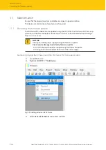
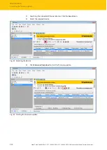
Page 37: ...ET DCP The following example shows the setting of the IP address via the Turck Service Tool The Turck Service Tool can be downloaded free of charge at www turck com Connect the device to a PC via the Ethernet interface Launch the Turck Service Tool Click Search or press F5 Fig 43 Turck Service Tool Start screen The Turck Service Tool displays the connected devices Fig 44 Turck Service Tool found d...

Page 38: ...com www turck com Fig 45 Turck Service Tool select the device to be addressed NOTE Clicking the IP address of the device opens the web server Change the IP address and if necessary the network mask and gateway Accept the changes by clicking Set in device Fig 46 Turck Service Tool Change device configuration ...

Page 39: ...ut filter and pulse stretch 2 0x02 PWM output EN_DO Activate output Kx 0 0x00 Yes Activates or deactivates the out put function of the digital chan nel 1 0x01 No IST Pulse stretching input 10 ms 0 254 0x00 0xFF Defines the duration of the pulse stretching for digital input edges from 10 to 2550 ms in multiples of 10 ms 10 pulse of 100 ms 0 pulse stretching deactivated SRO Manual reset after overcu...

Page 40: ...x01 smooth 1 Hz 0 25 Hz 2 0x02 fast 30 Hz 15 Hz 3 0x03 Off 250 Hz 125 Hz IMR Current range 0 0x00 4 20 mA 1 0x01 0 20 mA 2 0x02 20 20 mA OPM Operation mode 0 0x00 Thermocouple Selection of the operation mode for the respective channel If a channel is para meterized as voltage or current input the sensor supply is provided at pin 1 and 3 Thermocouples RTDs resistances must not be connected if the c...

Page 41: ...d junction compensation TCT Thermocouple type 0 0x00 Type K 270 1370 C 454 2498 F 1 0x01 Type B 100 1820 C 212 3308 F 2 0x02 Type E 270 1000 C 454 1832 F 3 0x03 Type J 210 1200 C 346 2192 F 4 0x04 Type N 270 1300 C 454 2372 F 5 0x05 Type R 50 1768 C 58 3214 F 6 0x06 Type S 50 1768 C 58 3214 F 7 0x07 Type T 270 400 C 454 752 F 8 0x08 Type C 0 2315 C 32 4199 F 9 0x09 Type G 0 2315 C 32 4199 F TMU Te...

Page 42: ...lue in case of a fieldbus error 1 0x01 Substitute value 2 0x02 Current value IRA Current range 0 0x00 0 20 mA Set the measurement range of the current out put 1 0x01 4 20 mA OPM Operation mode 0 0x00 Voltage The output is defined as a voltage output 1 0x01 Current The output is defined as a current output ORM Output recovery mode 0 0x00 Automatic The output switches on autmatically as soon as the ...

Page 43: ... outputs to 0 No error information sent 1 Hold current value The device maintains the actual out put data Deactivate all dia gnostics 0 No Diagnostic and alarm messages are generated 1 yes Diagnostic and alarm messages are suppressed Deactivate load voltage diagnostics 0 No The monitoring of voltage V2 is activ ated 1 yes The sending of the diagnosis is deac tivated Deactivate I O ASSIST ANT Force...

Page 44: ...TBEN S1 8DIP Word no Bit no 15 14 13 12 11 10 9 8 7 6 5 4 3 2 1 0 Inputs 0x0000 DI7 C7P4 DI6 C6P4 DI5 C5P4 DI4 C4P4 DI3 C3P4 DI2 C2P4 DI1 C1P4 DI0 C0P4 Diagnostics 0x0001 VERR V1 Ch4 7 VERR V1 Ch0 3 Latch input 0x0002 DI7 DI6 DI5 DI4 DI3 DI2 DI1 DI0 Counter Ch0 0x0003 Counter value LSB 0x0004 Counter value MSB Frequency Ch0 0x0005 Frequency MSB Frequency LSB Status 0x0006 Module status 0x0007 FCE ...

Page 45: ...4 Counter value MSB Frequency Ch0 0x0005 Frequency MSB Frequency LSB Status 0x0006 Module status 0x0007 FCE COM V1 ARGEE Diag Warn TBEN S2 8DIP Word no Bit no 15 14 13 12 11 10 9 8 7 6 5 4 3 2 1 0 Inputs 0x0000 DI7 C7P4 DI6 C6P4 DI5 C5P4 DI4 C4P4 DI3 C3P4 DI2 C2P4 DI1 C1P4 DI0 C0P4 Diagnostics 0x0001 VERR V1 C3 VERR V1 C2 VERR V1 C1 VERR V1 C0 Latch input 0x0002 DI7 DI6 DI5 DI4 DI3 DI2 DI1 DI0 Cou...

Page 46: ...ERR DO3 PWM Diagnostics Ch7 0x0002 PWM OUT ERR DO7 Module status 0x0003 FCE COM V1 ARGEE Diag Warn TBEN S1 4DIP 4DOP Word no Bit no 15 14 13 12 11 10 9 8 7 6 5 4 3 2 1 0 Inputs 0x0000 DI3 C3P4 DI2 C2P4 DI1 C1P4 DI0 C0P4 Diagnostics 0x0001 ERR3 ERR2 ERR1 ERR0 VERR V1 Ch4 7 VERR V1 Ch0 3 Latch input 0x0002 DI3 DI2 DI1 DI0 Counter Ch0 0x0003 Counter value LSB 0x0004 Counter value MSB Frequency Ch0 0x...

Page 47: ...DX0 C0P4 Diagnostics 0x0001 ERR3 ERR2 ERR1 ERR0 VERR V2 Ch2 3 VERR V1 Ch0 1 Latch input 0x0002 DX3 DX2 DX1 DX0 Counter Ch0 0x0003 Counter value LSB 0x0004 Counter value MSB Frequency Ch0 0x0005 Frequency MSB Frequency LSB Status 0x0006 PWM Diagnostics Ch3 0x0007 PWM OUT ERR DO3 Module status 0x0008 FCE COM V1 ARGEE Diag Warn ...

Page 48: ...5 C5P4 DX4 C4P4 DX3 C3P4 DX2 C2P4 DX1 C1P4 DX0 C0P4 Diagnostics 0x0001 ERR7 ERR6 ERR5 ERR4 ERR3 ERR2 ERR1 ERR0 VERR V2 Ch4 7 VERR V1 Ch0 3 Latch input 0x0002 DX7 DX6 DX5 DX4 DX3 DX2 DX1 DX0 Counter Ch0 0x0003 Counter value LSB 0x0004 Counter value MSB Frequency Ch0 0x0005 Frequency MSB Frequency LSB Status 0x0006 PWM Diagnostics Ch3 0x0007 PWM OUT ERR DO3 PWM Diagnostics Ch7 0x0008 PWM OUT ERR DO7...

Page 49: ...unter value MSB Frequency Ch0 0x0005 Frequency MSB Frequency LSB Status 0x0006 PWM Diagnostics Ch3 0x0007 PWM OUT ERR DO3 PWM Diagnostics Ch7 0x0008 PWM OUT ERR DO7 Module status 0x0009 FCE COM V1 ARGEE Diag Warn Meaning of process data bits Name Meaning I O data Cx Connector x DIx Digital input x DOx Digital input x DXx DXP channel x DXx Latch input The input values ind the in put bits are hold a...

Page 50: ...UX1 at the channel channels VERR V1 Cx Overcurrent VAUX1 at the connector VERR V2 Ch xy Overcurrent VAUX2 at the channel channels ERRx Overcurrent at output PWM Diagnostics PWM OUT ERR DOx Overcurrent at the PWM output Module status COM Device internal communication disturbed DiagWarn Diagnostic message at the device FCE Force Mode activated V1 System power supply too low 18 VDC V2 V2 too low 18 V...

Page 51: ...2 LLVU UFL OFL WBR V1 AOL ULVE RTDSC CJE LLVU UFL OFL WBR V1 AOL ULVE RTDSC CJE Module status 0x0006 FCE COM V1 ARGEE Diag Warn TBEN S2 4AO Word no Bit no 15 14 13 12 11 10 9 8 7 6 5 4 3 2 1 0 Diagnostics 0x0000 Channel 1 Channel 0 WBR OVL WBR OVL 0x0001 Channel 3 Channel 2 WBR OVL WBR OVL Module status 0x0002 FCE COM V1 ARGEE Diag Warn Meaning of the process data bits Name Meaning CJE Cold juncti...

Page 52: ...ies far below the Nominal range thresholds see 182 Resistance thermocouple RTD Not valid ULVE Upper limit value ex ceeded Current voltage resistance The measured value lies above the Nominal range thresholds see 182 Thermocouple RTD The measured temperature lies more than 1 above the nominal range V1AOL Overcurrent VAUX1 The sensor supply is not within the permissible range WBR Wire break TBEN S2 ...

Page 53: ...DI7 DI6 DI5 DI4 DI3 DI2 DI1 DI0 Counter reset 0x0002 CNT_ Reset TBEN S1 8DIP D Word no Bit no 15 14 13 12 11 10 9 8 7 6 5 4 3 2 1 0 Control 0x0000 Latch reset 0x0001 DI7 DI6 DI5 DI4 DI3 DI2 DI1 DI0 Counter reset 0x0002 CNT_ Reset TBEN S2 8DIP D Word no Bit no 15 14 13 12 11 10 9 8 7 6 5 4 3 2 1 0 Control 0x0000 Latch reset 0x0001 DI7 DI6 DI5 DI4 DI3 DI2 DI1 DI0 Counter reset 0x0002 CNT_ Reset ...

Page 54: ...1 DO0 PWM ch3 0x0002 Duty Cycle PWM ch7 0x0003 Duty Cycle TBEN S1 4DIP 4DOP Word no Bit no 15 14 13 12 11 10 9 8 7 6 5 4 3 2 1 0 Control 0x0000 Outputs 0x0001 DO7 DO6 DO5 DO4 Latch reset 0x0002 DI3 DI2 DI1 DI0 Counter reset 0x0003 CNT_ Reset PWM ch7 0x0004 Duty Cycle TBEN S1 4DXP Word no Bit no 15 14 13 12 11 10 9 8 7 6 5 4 3 2 1 0 Control 0x0000 Outputs 0x0001 DX3 DX2 DX1 DX0 Latch reset 0x0002 D...

Page 55: ... Word no Bit no 15 14 13 12 11 10 9 8 7 6 5 4 3 2 1 0 Control 0x0000 Outputs 0x0001 DX7 DX6 DX5 DX4 DX3 DX2 DX1 DX0 Latch reset 0x0002 DX7 DX6 DX5 DX4 DX3 DX2 DX1 DX0 Counter reset 0x0003 CNT_ Reset PWM ch3 0x0004 Duty Cycle PWM ch7 0x0005 Duty Cycle VAUX Control 0x0006 VAUX2 P1 C3 VAUX2 P1 C2 VAUX1 P1 C1 VAUX1 P1 C0 Meaning of the process data bits Name Meaning I O data DIx Latch reset bit for in...

Page 56: ... back to 0 and starts a new count operation P1 Pin 1 Duty Cycle Mark to space ratio 10 90 VAUX1 P1 C1 Switches the sensor actuator supply at pin 1 of the connector 8 3 2 Process output data analog modules TBEN S2 4AO Word no Bit no 15 14 13 12 11 10 9 8 7 6 5 4 3 2 1 0 Control 0x0000 Outputs 0x0001 Analog value channel 0 0x0002 Analog value channel 1 0x0003 Analog value channel 2 0x0004 Analog val...

Page 57: ...cation of the slots and sub slots and thus the assignment of functions operation mode diagnostics etc is done in the configuration software of the PROFINET controller This device model allows manufacturers to design modular and flexible decentral field devices Users are flexible in con figuring decentralized field devices Fig 47 TIA Portal assignment of the slots and sub slots on the example of an...

Page 58: ...rated by a period A name component i e a string between two dots may be a maximum of 63 characters long n The device name must not start or end with a hyphen n The device name must not start with port xyz y z 0 9 n The name must not have the form of an IP address n n n n 0 999 n Do not use special characters n Do not use capital letters 8 4 3 FSU Fast Start Up prioritized startup FSU enables a PLC...

Page 59: ...or example in TIA Portal Siemens Autonegotiation deactivated Transmission medium duplex set to a fixed value Please observe during configuration that the neighboring devices do also support FSU and that the settings for the ports of neighboring devices are identical Set Transmission rate duplex to a fix value Deactivate auto negotiation Fig 48 TIA Portal port settings for FSU ...

Page 60: ...figuring devices at PROFINET 60 Hans Turck GmbH Co KG T 49 208 4952 0 F 49 208 4952 264 more turck com www turck com Activate the prioritized start up at the I O device Fig 49 TIA Portal prioritized start up activation at the I O device ...

Page 61: ...re an application must be able to com pensate for the 200 ms interruption The reconfiguration time always depends on the Media Redundancy Manager e g the PROFINET PLC and the I O cycle and watchdog times set here For PROFINET the response monitoring time must be selected accordingly 200 ms It is not possible to use Fast Start Up in an MRP network 8 4 5 User data for acyclic services The acyclic da...

Page 62: ...ion Maintaining 45041 0xAFF1 I M0 functions STRING 54 read write I M Tag function and location 45042 0xAFF2 I M2 functions STRING 16 read write I M Installation Date 45043 0xAFF3 I M3 functions STRING 54 read write I M Description Text 45044 0xAFF4 I M4 functions STRING 54 read write I M Signature 45045 45055 0xAFF5 0xAFFF I M5 to I M15 functions not supported Acyclic I O channel user data Index N...

Page 63: ...V04 00 2021 05 63 Index Name Data Type Access Comment 20 22 0x14 0x16 reserved 23 0x17 Output data specific read write Output data of the respect ive I O channel reserved ...

Page 64: ...components are used in this example n Siemens PLC S7 1500 n TBEN S block module Used software The following software tools are used in this example n SIMATIC STEP7 Professional V13 TIA Portal n GSDML file for TBEN S can be downloaded for free as ZIP archive TBEN S_PROFINET zip under www turck com Prerequisites n The programming software has been started n A new project has been created n The PLC h...

Page 65: ... 2021 05 65 Installing the GSDML file Define the storage location of the GSDML file and click Install a The device is added to the Hardware catalog of the programming software Fig 51 Installing the GSDML file ...

Page 66: ...KG T 49 208 4952 0 F 49 208 4952 264 more turck com www turck com 8 5 2 Connecting the devices to the PLC Select the TBEN S devices from the Hardware catalog and drag them into the Device networks editor Connect the devices to the PLC in the Devices networks editor Fig 52 Connecting the device to the PLC ...

Page 67: ...Configuring device functions Select Device view Ò Device overview Select functions as operation mode diagnostics etc from the hardware catalog and add them to the devoce slots via drag drop Fig 53 Configuring the device slots ...

Page 68: ... GmbH Co KG T 49 208 4952 0 F 49 208 4952 264 more turck com www turck com 8 5 4 Assigning the PROFINET device name Select Online access Ò Online diagnostics Functions Ò Assign PROFINET device name Assign the desired PROFINET device name with Assign name Fig 54 Assigning the PROFINET device name ...

Page 69: ...V04 00 2021 05 69 8 5 5 Setting the IP address in TIA Portal Select Device view Ò Properties Ò Ethernet addresses Assign the desired IP address Fig 55 Assigning the IP address ...

Page 70: ...Turck GmbH Co KG T 49 208 4952 0 F 49 208 4952 264 more turck com www turck com 8 5 6 Setting module parameters Select Device view Ò Device overview Select the device to be parameterized Click Properties Ò General Ò Module parameters Set the device parameters Fig 56 Setting module parameters ...

Page 71: ...de Go online a The device has been successfully connected to the PLC Fig 57 Starting the online mode 8 5 8 PROFINET Mapping The PROFINET mapping corresponds to the data mapping described in the sections Evaluating Process Input Data 44 and Writing Process Output Data 53 ...

Page 72: ...nly Process data of inputs identical to registers 0x8000 0x8FFF 0x0800 0x09FF read write Process data of the outputs identical to registers 0x9000 0x9FFF 0x1000 0x100B read only Module identifier 0x100C read only Module status 0x1017 read only Register mapping revision always 2 if not mapping is incompatible with this description 0x1020 read only Watchdog actual time in ms 0x1120 read write Watchd...

Page 73: ...2 44097 44103 404097 404103 Module status 0x100C 4108 44109 404109 Watchdog actual time 0x1020 4128 44129 404129 Watchdog pre defined time 0x1120 4384 44385 404385 Modbus connec tion mode re gister 0x1130 4400 44401 404401 Modbus Connec tion Timeout in sec 0x1131 4401 44402 404402 Modbus Para meter Restore 0x113C 0x113D 4412 4413 44413 44414 404413 404414 Modbus Para meter Save 0x113E 0x113F 4414 ...

Page 74: ...ction is already opened during the connection establishment The first Mod bus connection thus receives the write author ization all following connections don t only if bit 0 1 2 15 reserved Register 0x1131 Modbus connection timeout This register defines after which time of inactivity a Modbus connection is closed through a Dis connect Value range 0 65535 s default 0 s never Modbus connection will ...

Page 75: ...unction codes FC16 and FC23 a The parameters are saved 8 6 3 Data width of the I O modules The following table shows the data width of the TBEN S modules within the Modbus register area and the type of data alignment Module Process input data Process output data Alignment TBEN S1 8DIP 8 bit Bit by bit TBEN S2 8DIP 8 bit Bit by bit TBEN S1 8DIP D 8 bit Bit by bit TBEN S1 8DOP 8 bit Bit by bit TBEN ...

Page 76: ...DI7 C7P4 DI6 C6P4 DI5 C5P4 DI4 C4P4 DI3 C3P4 DI2 C2P4 DI1 C1P4 DI0 C0P4 Diagn 0x0001 VERR V1 Ch4 7 VERR V1 Ch0 3 Latch IN 0x0002 DI7 DI6 DI5 DI4 DI3 DI2 DI1 DI0 CNT Ch0 0x0003 Counter value LSB 0x0004 Counter value MSB Freq Ch0 0x0005 Frequency MSB Frequency LSB Status 0x0006 Module status 0x0007 FCE COM V1 ARGEE Diag Warn TBEN S1 8DIP output registers Meaning of the process output data 53 Registe...

Page 77: ...sters Meaning of the process input data 44 Register no Bit no 15 14 13 12 11 10 9 8 7 6 5 4 3 2 1 0 IN 0x0000 DI7 C7P4 DI6 C6P4 DI5 C5P4 DI4 C4P4 DI3 C3P4 DI2 C2P4 DI1 C1P4 DI0 C0P4 Diagn 0x0001 VERR V1 C7 VERR V1 C6 VERR V1 C5 VERR V1 C4 VERR V1 C3 VERR V1 C2 VERR V1 C1 VERR V1 C0 Latch IN 0x0002 DI7 DI6 DI5 DI4 DI3 DI2 DI1 DI0 CNT K0 0x0003 Counter value LSB 0x0004 Counter value MSB Freq Ch0 0x0...

Page 78: ...ss output data 53 Register no Bit no 15 14 13 12 11 10 9 8 7 6 5 4 3 2 1 0 Latch reset 0x0800 DI7 DI6 DI5 DI4 DI3 DI2 DI1 DI0 Counter reset 0x0801 CNT reset TBEN S1 8DIP D parameter registers Parameter description 39 Register no Bit no 15 14 13 12 11 10 9 8 7 6 5 4 3 2 1 0 Channel 0 0xB000 IST DI0 DIFT DI0 DMOD_CNT DI0 Channel 1 0xB001 IST DI1 DIFT DI1 DMOD DI1 Channel 7 0xB007 IST DI7 DIFT DI7 DM...

Page 79: ...ERR V1 C2 VERR V1 C1 VERR V1 C0 Latch IN 0x0002 DI7 DI6 DI5 DI4 DI3 DI2 DI1 DI0 CNT Ch0 0x0003 Counter value LSB 0x0004 Counter value MSB Freq Ch0 0x0005 Frequency MSB Frequency LSB Status 0x0006 Module status 0x0007 FCE COM V1 ARGEE Diag Warn TBEN S2 8DIP output registers Meaning of the process output data 53 Register no Bit no 15 14 13 12 11 10 9 8 7 6 5 4 3 2 1 0 Latch reset 0x0800 DI7 DI6 DI5 ...

Page 80: ...com TBEN S2 8DIP parameter registers Parameter description 39 Register no Bit no 15 14 13 12 11 10 9 8 7 6 5 4 3 2 1 0 Channel 0 0xB000 IST DI0 DIFT DI0 DMOD_CNT DI0 Channel 1 0xB001 IST DI1 DIFT DI1 DMOD DI1 Channel 7 0xB007 IST DI7 DIFT DI7 DMOD DI7 VAUX 0xB009 VAUX1 Pin1 C1 Ch2 3 VAUX1 Pin1 C0 Ch0 1 0xB00A VAUX1 Pin1 C3 Ch6 7 VAUX1 Pin1 C2 Ch4 5 ...

Page 81: ...RGEE Diag Warn TBEN S1 8DOP output registers Meaning of the process output data 53 Register no Bit no 15 14 13 12 11 10 9 8 7 6 5 4 3 2 1 0 OUT 0x0800 DO7 C7P4 DO6 C6P4 DO5 C5P4 DO4 C4P4 DO3 C3P4 DO2 C2P4 DO1 C1P4 DO0 C0P4 PWM Ch3 0x0801 Duty Cycle PWM Ch7 0x0802 Duty Cycle TBEN S1 8DOP parameter registers Parameter description 39 Register no Bit no 15 14 13 12 11 10 9 8 7 6 5 4 3 2 1 0 Channel 0 ...

Page 82: ... ERR3 ERR2 ERR1 ERR0 VERR V1 Ch4 7 VERR V1 Ch0 3 Latch IN 0x0002 DI3 DI2 DI1 DI0 CNT Ch0 0x0003 Counter value LSB 0x0004 Counter value MSB Freq Ch0 0x0005 Frequency MSB Frequency LSB Status 0x0006 PWM diag Ch7 0x0007 PWM OUT ERR Module status 0x0008 FCE COM V1 ARGEE Diag Warn TBEN S1 4DIP 4DOP output registers Meaning of the process output data 53 Register no Bit no 15 14 13 12 11 10 9 8 7 6 5 4 3...

Page 83: ...D DI2 Channel 3 0xB004 IST DI3 DIFT DI3 DMOD DI3 Channel 7 0xB005 DMOD_PWM DO7 TBEN S1 4DXP input registers Meaning of the process input data 44 Register no Bit no 15 14 13 12 11 10 9 8 7 6 5 4 3 2 1 0 IN 0x0000 DX3 C3P4 DX2 C2P4 DX1 C1P4 DX0 C0P4 Diagn 0x0001 ERR3 ERR2 ERR1 ERR0 VERR V2 Ch2 3 VERR V1 Ch0 1 Latch IN 0x0002 DX3 DX2 DX1 DX0 CNT Ch0 0x0003 Counter value LSB 0x0004 Counter value MSB F...

Page 84: ... 13 12 11 10 9 8 7 6 5 4 3 2 1 0 OUT 0x0800 DX3 C3P4 DX2 C2P4 DX1 C1P4 DX0 C0P4 Latch reset 0x0801 DX3 DX2 DX1 DX0 CNT reset 0x0802 CNT reset PWM Ch3 0x0803 Duty Cycle TBEN S1 4DXP parameter registers Parameter description 39 Register no Bit no 15 14 13 12 11 10 9 8 7 6 5 4 3 2 1 0 Channel 0 channel 7 0xB000 EN DO3 EN DO2 EN DO1 EN DO0 SRO3 SRO2 SRO1 SRO0 Channel 0 0xB001 IST DX0 DIFT DX0 DMOD_CNT...

Page 85: ...0 0x0003 Counter value LSB 0x0004 Counter value MSB Freq Ch0 0x0005 Frequency MSB Frequency LSB Status 0x0006 PWM diag Ch 3 0x0007 PWM OUT ERR PWM diag Ch7 0x0008 PWM OUT ERR Module status 0x0009 FCE COM V1 ARGEE Diag Warn TBEN S1 8DXP output registers Meaning of the process output data 53 Register no Bit no 15 14 13 12 11 10 9 8 7 6 5 4 3 2 1 0 OUT 0x0800 DX7 C7P4 DX6 C6P4 DX5 C5P4 DX4 C4P4 DX3 C...

Page 86: ...hannel 7 0xB000 EN DO7 EN DO6 EN DO5 EN DO4 EN DO3 EN DO2 EN DO1 EN DO0 SRO7 SRO6 SRO5 SRO4 SRO3 SRO2 SRO1 SRO0 Channel 0 0xB001 IST DX0 DIFT DX0 DMOD_CNT DX0 Channel 1 0xB002 IST DX1 DIFT DX1 DMOD DX1 Channel 2 0xB003 IST DX2 DIFT DX2 DMOD DX2 Channel 3 0xB004 IST DX3 DIFT DX3 DMOD_PWM DX3 0xB005 Channel 4 0xB006 IST DX4 DIFT DX4 DMOD DX4 Channel 5 0xB007 IST DX5 DIFT DX5 DMOD DX5 Channel 6 0xB00...

Page 87: ... DX0 C0P4 Diagn 0x0001 ERR7 ERR6 ERR5 ERR4 ERR3 ERR2 ERR1 ERR0 VERR V2 P1 Ch6 7 VERR V2 P1 Ch4 5 VERR V1 P1 Ch2 3 VERR V1 P1 Ch0 1 Latch IN 0x0002 DX7 DX6 DX5 DX4 DX3 DX2 DX1 DX0 CNT Ch0 0x0003 Counter value LSB 0x0004 Counter value MSB Freq Ch0 0x0005 Frequency MSB Frequency LSB Status 0x0006 PWM diag Ch 3 0x0007 PWM OUT ERR DO3 PWM diag Ch7 0x0008 PWM OUT ERR DO7 Module status 0x0009 FCE COM V1 ...

Page 88: ...rs Meaning of the process output data 53 Register no Bit no 15 14 13 12 11 10 9 8 7 6 5 4 3 2 1 0 OUT 0x0800 DX7 C3P2 DX6 C3P4 DX5 C2P2 DX4 C2P4 DX3 C2P2 DX2 C1P4 DX1 C0P2 DX0 C0P4 Latch reset 0x0801 DX7 DX6 DX5 DX4 DX3 DX2 DX1 DX0 CNT reset 0x0802 CNT reset PWM Ch7 0x0803 Duty Cycle PWM Ch7 0x0804 Duty Cycle VAUX Control 0x0805 VAUX 1 P1 C3 VAUX 1 P1 C2 VAUX 1 P1 C1 VAUX 1 P1 C0 ...

Page 89: ...el 0 0xB001 IST DX0 DIFT DX0 DMOD_CNT DX0 Channel 1 0xB002 IST DX1 DIFT DX1 DMOD DX1 Channel 2 0xB003 IST DX2 DIFT DX2 DMOD DX2 Channel 3 0xB004 IST DX3 DIFT DX3 DMOD_PWM DX3 0xB005 Channel 4 0xB006 IST DX4 DIFT DX4 DMOD DX4 Channel 5 0xB007 IST DX5 DIFT DX5 DMOD DX5 Channel 6 0xB008 IST DX6 DIFT DX6 DMOD DX6 Channel 7 0xB009 IST DX7 DIFT DX7 DMOD_PWM DX7 0xB00A VAUX 0xB00B VAUX1 Pin1 C1 Ch2 3 VAU...

Page 90: ...Channel 2 0x0005 LLVU UFL OFL WBR V1 AOL ULVE RTD SC CJE LLVU UFL OFL WBR V1 AOL ULVE RTD SC CJE Module status 0x0006 FCE COM V1 ARGEE Diag Warn TBEN S2 4AI parameter registers Parameter description 39 Register no Bit no 15 14 13 12 11 10 9 8 7 6 5 4 3 2 1 0 Channel 0 0xB000 INFIL DRE DCH DDI OPM TMU SUP 0xB001 RTDWT RRA RWT CWT IMR VWT UMR 0xB002 TCT TCCCJ RTDT Channel 1 0xB003 INFIL DRE DCH DDI ...

Page 91: ...agnostics Channel 1 Channel 0 0x0000 WBR OVL WBR OVL Channel 3 Channel 2 0x0001 WBR OVL WBR OVL Module status 0x0002 FCE COM V1 ARGEE Diag Warn TBEN S2 4AO output registers Meaning of the process output data 56 Register no Bit no 15 14 13 12 11 10 9 8 7 6 5 4 3 2 1 0 AO0 0x0800 MSB LSB AO1 0x0801 MSB LSB AO2 0x0802 MSB LSB AO3 0x0803 MSB LSB ...

Page 92: ...hannel 3 0xB009 ORM DRE DCH DDI OPM FFB 0xB00A URA IRA 0xB00B SVAL MSB SVAL LSB 8 6 5 Meaning of the register bits Designation Meaning In output data AI Analog input AO Analog output C Connector DI Digital input DO Digital output DX DXP channel P Pin Module status ARGEE ARGEE program running in the device COM Device internal communication disturbed DiagWarn Diagnostics available at the device FCE ...

Page 93: ...RO Manual reset after overcurrent VAUX1 Pin1 Cx Chy z Sensor actuator supply VAUX1 Analog modules TBEN S2 4AI CWT Current wiring type DCH Deactivate channel DDI Deactivate diagnostics DRE Data representation INFL Input averaging filter IMR Current range OPM Operation mode RRA Resistance range RTDT RTD type RTDWT RTD wiring type RWT Resistance wiring type SUP Mains suppression TCCCJ Thermocouple co...

Page 94: ...in the actual value in case of an error 0 ms default 500 ms Outputs switch to 0 after the watchdog time has expired setting in re gister 0x1120 NOTE Setting the outputs to predefined substitute values is not possible in Modbus TCP Eventually parameterized substitute values will not be used Behavior of the BUS LED If the watchdog triggers the BUS LED behaves as follows Watchdog BUS LED Tripped Red ...

Page 95: ...507 P3CV01 Modbus TCP Master IP address 192 168 1 15 n Block module TBEN S1 4DIP 4DOP IP address 192 168 201 Used software The following software tools are used in this example n CODESYS 3 5 8 1 can be dwonloaded for free under www turck com Prerequisites n The programming software has been started n A new project has been created n The PLC has been added to the project ...

Page 96: ... 0 F 49 208 4952 264 more turck com www turck com 8 7 1 Connecting the device to the PLC The following components have to be added to CODESYS first in order to connect the device to the PLC n Ethernet Adapter n Modbus TCP Master n Modbus TCP Slave Adding the Ethernet adapter Right click the Device TX507 P3CV01 Fig 58 Project tree ...

Page 97: ...V04 00 2021 05 97 Select Add Device Select the Ethernet Adapter Click Add Device a The Ethernet Adapter is added to the project tree as Ethernet Ethernet Fig 59 Adding the Ethernet adapter ...

Page 98: ...k GmbH Co KG T 49 208 4952 0 F 49 208 4952 264 more turck com www turck com Adding the Modbus master Right click the Ethernet Ethernet in the project tree Select Add Device Double click Modbus TCP Master a The Modbus Master is added to the project tree as Modbus_TCP_Master Fig 60 Adding the Modbus master ...

Page 99: ...ding a Modbus slave Right click the Modbus TCP Master in the project tree Select Add Device Double click the Modbus TCP Slave a The Modbus Slave is added to the project tree as Modbus_TCP_Slave Fig 61 Adding a Modbus slave ...

Page 100: ... TCP master 100 Hans Turck GmbH Co KG T 49 208 4952 0 F 49 208 4952 264 more turck com www turck com 8 7 2 Configuring the network interface Click DeviceÒ Scan Network Modbus Master here TX507 P3CV01 and confirm with OK Fig 62 Configuring the network interface to the Modbus master ...

Page 101: ... 05 101 Double click Ethernet Open the dialog box Network Adapter by clicking the button in the register tab General Select the interfac of the TX507 here 192 168 1 15 Fig 63 Modbus master selecting the interface ...

Page 102: ... Hans Turck GmbH Co KG T 49 208 4952 0 F 49 208 4952 264 more turck com www turck com 8 7 3 Modbus TCP slave configuring the IP address Double click the Modbus TCP Slave Enter the slave s IP address in the General register tab here 192 268 1 201 Fig 64 Modbus TCP slave configuring the IP address ...

Page 103: ...el 0 input data Double click the Modbus TCP Slave In the register tab Modbus Slave Channel select Add Channel Enter the following values Channel name Access type Read Input Registers Offset 0x0000 Length 1 register Confirm with OK Fig 65 Defining the input register ...

Page 104: ...2 0 F 49 208 4952 264 more turck com www turck com Defining channel 1 output data Double click the Modbus TCP Slave In the register tab Modbus Slave Channel select Add Channel Enter the following values Channel name Access type Write Singe Register Offset 0x0000 Length 1 register Confirm with OK Fig 66 Defining the output register ...

Page 105: ...process data The process data can be interpreted by means of the mapping 76 if the device is connected to the PLC Double click the Modbus TCP Slave Click the register tab ModbusTCP Slave I O Mapping Set the function Alway update variables to Activated 1 a The process data are displayed Fig 67 Process data ...

Page 106: ...onnect enables a PLC to build up connections to EtherNet IP nodes in less than 500 ms after switching on the power supply for the EtherNet IP network The fast start up is necessary for fast tool changing applications at robot arms for ex ample in the automobile industry The devices support QuickConnect The function can only be guaranteed for the digital chan nels QuickConnect can be activated via ...

Page 107: ...guring the Configuration Assembly in RSLogix Activate QuickConnect via byte 9 bit 0 1 in the Controller Tags Fig 68 Configuring QuickConnect in RSLogix Activating Quick Connect via Class Instance Attribute Activate Quick Connect via Class Instance Attribute as follows Class Instance Attribute Value 0xF5 0x01 0x0C 0 deactivated default 1 activated ...

Page 108: ...ce Level Ring DLR redundancy protocol is used to increase the stability of EtherNet IP networks DLR enabled devices have an integrated switch and can thus be integrated into a ring topology The DLR protocol is used to detect an interruption in the ring If the data line ins interrupted data are sent through an alternative network section so that the network can be reconfigured as soon as possible D...

Page 109: ...therNet IP offer the possibility of mapping diagnostic data into the process data The diagnostic messages are directly mapped into the process data Additionally the device s status word contains the mod ule diagnostics The status word contains the module status Byte no Bit no 7 6 5 4 3 2 1 0 0 LSB Under voltage V2 Module dia gnostics pending 1 MSB Force Mode active Under voltage V1 Control word Th...

Page 110: ...ed to the Turck products Instance attributes Attribute no Attribute name Get set Type Value Dec Hex 1 0x01 Vendor ID G UINT Contains the manufacturer ID Turck 0x46 2 0x02 Product type G UINT Shows the general product type Communications Adapter 12dez 0x0C 3 0x03 Product code G UINT Identifies a special product in a device type default 27247dec 6A6F 4 0x04 Revision n Major n Minor G STRUCT OF n USI...

Page 111: ...x0E Yes Yes Get_Attribute_Single returns the content of a specified attribute 16 0x10 No No Set_Attribute_Single changes a single attribute Assembly Object 0x04 Assembly Objects bind attributes of multiple objects to allow data to or from each object to be sent or received over a single connection The following description of the Ethernet Link Object is taken from the CIP specification Vol 2 Rev 2...

Page 112: ...ibute Configuration Assembly Instance 106 The modules support Configuration Assembly The Configuration Assembly contains 10 bytes module configuration data EtherNet IP specific x Byte parameter data depending on device type Device Configuration Data The default values are written in bold Designation Value Meaning QuickConnect 0 disabled QuickConnect is deactivated 1 Activated QuickConnect is activ...

Page 113: ...t Setup Eth1 Port Setup Quick Connect Parameter data 39 Channel 0 10 0x0A DMOD_CNT DI0 11 0x0B DIFT DI0 12 0x0C IST DI0 13 0x0D Channel 1 14 0x0E DMOD DI1 15 0x0F DIFT DI1 16 0x10 IST DI1 17 0x11 Channel 2 18 0x12 Assignment similar to channel 1 byte 14 17 19 0x13 20 0x14 21 0x15 Channel 7 38 0x26 Assignment similar to channel 1 byte 14 17 39 0x27 40 0x28 41 0x29 ...

Page 114: ...h2 Port Setup Eth1 Port Setup Quick Connect Parameter data 39 Channel 0 10 0x0A DMOD_CNT DI0 11 0x0B DIFT DI0 12 0x0C IST DI0 13 0x0D Channel 1 14 0x0E DMOD DI1 15 0x0F DIFT DI1 16 0x10 IST DI1 17 0x11 Channel 2 18 0x12 Assignment similar to channel 1 byte 14 17 19 0x13 20 0x14 21 0x15 Channel 7 38 0x26 Assignment similar to channel 1 byte 14 17 39 0x27 40 0x28 41 0x29 42 0x2A VAUX1 pin1 C0 Ch0 1 ...

Page 115: ...E DMOD_PWM channel 7 n Configuration Assembly TBEN S1 4DIP 4DOP Byte no Bit no Dec Hex 7 6 5 4 3 2 1 0 Device Configuration Data 112 0 9 0x00 0x09 Eth2 Port Setup Eth1 Port Setup Quick Connect Parameter data 39 10 0x0A SRO7 SRO6 SRO5 SRO4 11 0x0B 12 0x0C DMOD_CNT DI0 13 0x0D DIFT DI0 14 0x0E IST DI0 15 0x0F 16 0x10 DMOD_DI1 17 0x11 DIFT DI1 18 0x12 IST DI1 19 0x13 20 0x14 DMOD_DI2 21 0x15 DIFT DI2...

Page 116: ... 6 5 4 3 2 1 0 Device Configuration Data 112 0 9 0x00 0x09 Eth2 Port Setup Eth1 Port Setup QuickCon nect Parameter data 39 10 0x0A SRO3 SRO2 SRO1 SRO0 11 0x0B EN DO3 EN DO2 EN DO1 EN DO0 12 0x0C DMOD_CNT DX0 13 0x0D DIFT DX0 14 0x0E IST DX0 15 0x0F 16 0x10 DMOD_DX1 17 0x11 DIFT DX1 18 0x12 IST DX1 19 0x13 20 0x14 DMOD_DX2 21 0x15 DIFT DX2 22 0x16 IST DI2 23 0x17 24 0x18 DMOD_DX3 25 0x19 DIFT DX3 2...

Page 117: ...N DO3 EN DO2 EN DO1 EN DO0 12 0x0C DMOD_CNT DX0 13 0x0D DIFT DX0 14 0x0E IST DX0 15 0x0F 16 0x10 DMOD_DX1 17 0x11 DIFT DX1 18 0x12 IST DX1 19 0x13 20 0x14 DMOD_DX2 21 0x15 DIFT DX2 22 0x16 IST DI2 23 0x17 24 0x18 DMOD_DX3 25 0x19 DIFT DX3 26 0x1A IST DX3 27 0x1B 28 0x1C DMOD_DX4 29 0x1D DIFT DX4 30 0x1E IST DX4 31 0x1F 32 0x20 DMOD_DX5 33 0x21 DIFT DX5 34 0x22 IST DX5 35 0x23 36 0x24 DMOD_DX6 37 0...

Page 118: ... DX0 28 0x1C IST DX0 29 0x1D 30 0x1E DMOD_DX1 31 0x1F DIFT DX1 32 0x20 IST DX1 33 0x21 34 37 0x22 0x25 Parameters DX2 assignment acc to byte 30 33 0x1E 0x21 for DX1 38 0x26 DMOD_PWM DX3 39 0x27 DIFT DX3 40 0x28 IST DX3 41 0x29 42 45 0x2A 0x2D Parameters DX4 assignment acc to byte 30 33 0x1E 0x21 for DX1 46 49 0x2E 0x31 Parameters DX5 assignment acc to byte 30 33 0x1E 0x21 for DX1 50 53 0x32 0x35 P...

Page 119: ...iring type 15 0x0F Current range 16 0x10 Current wiring type 17 0x11 Resistance range 18 0x12 Resistance wiring type 19 0x13 RTD type 20 0x14 RTD wiring type 21 0x15 Data representation 22 0x16 Temp unit 23 0x17 Input averaging filter DIFT 24 0x18 Deactiv ch 25 0x19 Deactivate diagn 26 0x1A Mains sup pression 27 0x1B Channel 1 28 45 0x1C 0x2D Assignment similar to channel 0 byte 10 27 Channel 2 46...

Page 120: ...k Connect Parameter data 39 Channel 0 10 0x0A Operation mode 11 0x0B Current range 12 0x0C Data representation 13 0x0D Voltage range 14 0x0E Deactiv ch 15 0x0F Output recovery mode 16 0x10 Deactivate diagn 17 0x11 Output on fieldbus error 18 0x12 Substitute value SVAL 19 0x13 Channel 1 20 29 0x14 0x1D Assignment similar to channel 0 byte 10 19 Channel 2 30 39 0x1E 0x27 Assignment similar to channe...

Page 121: ...nstance 103 and Instance 104 Instance 103 and Instance 104 are in and output assembly instances with variable assembly sizes The assembly size is pre calculated to support the device s I O configuration enabled dia gnostics etc The effective size of the Assembly Instance can be determined using the As sembly Object instance 0 67 attribute 0x04 Input data Input Assembly Instance 103 0 470 bytes def...

Page 122: ...7 words Word no Bit no 15 14 13 12 11 10 9 8 7 6 5 4 3 2 1 0 Status 0x0000 FCE COM V1 ARGEE Diag Warn IN 0x0001 DI7 C7P4 DI6 C6P4 DI5 C5P4 DI4 C4P4 DI3 C3P4 DI2 C2P4 DI1 C1P4 DI0 C0P4 Diagn 0x0002 VERR V1 Ch4 7 VERR V1 Ch0 3 Latch IN 0x0003 DI7 DI6 DI5 DI4 DI3 DI2 DI1 DI0 CNT Ch0 0x0004 Counter value LSB 0x0005 Counter value MSB Freq Ch0 0x0006 Frequency MSB Frequency LSB Module status 0x0007 n Ou...

Page 123: ...DI0 C0P4 Diagn 0x0002 VERR V1 C3 VERR V1 C2 VERR V1 C1 VERR V1 C0 Latch IN 0x0003 DI7 DI6 DI5 DI4 DI3 DI2 DI1 DI0 CNT Ch0 0x0004 Counter value LSB 0x0005 Counter value MSB Freq Ch0 0x0006 Frequency MSB Frequency LSB Module status 0x0007 n Output data TBEN S2 8DIP 53 Control word 2 words Word no Bit no 15 14 13 12 11 10 9 8 7 6 5 4 3 2 1 0 Control 0x0000 Latch reset 0x0001 DI7 DI6 DI5 DI4 DI3 DI2 D...

Page 124: ... C5P4 DI4 C4P4 DI3 C3P4 DI2 C2P4 DI1 C1P4 DI0 C0P4 Deactivate diagn 0x0002 VERR V1 C7 VERR V1 C6 VERR V1 C5 VERR V1 C4 VERR V1 C3 VERR V1 C2 VERR V1 C1 VERR V1 C0 Latch IN 0x0003 DI7 DI6 DI5 DI4 DI3 DI2 DI1 DI0 CNT Ch0 0x0004 Counter value LSB 0x0005 Counter value MSB Freq Ch0 0x0006 Frequency MSB Frequency LSB Module status 0x0007 n Output data TBEN S1 8DIP D 53 control word 2 words Word no Bit n...

Page 125: ...RR6 ERR5 ERR4 ERR3 ERR2 ERR1 ERR0 VERR V2 Ch4 7 VERR V2 Ch0 3 PWM diag Ch 3 0x0002 PWM OUT ERR DO3 PWM diag Ch7 0x0003 PWM OUT ERR DO7 n Output data TBEN S1 8DOP 53 control word 3 words Word no Bit no 15 14 13 12 11 10 9 8 7 6 5 4 3 2 1 0 Control 0x0000 OUT 0x0001 DO7 C7P4 DO6 C6P4 DO5 C5P4 DO4 C4P4 DO3 C3P4 DO2 C2P4 DO1 C1P4 DO0 C0P4 PWM Ch3 0x0002 Duty Cycle PWM Ch7 0x0003 Duty Cycle ...

Page 126: ...ord 8 words Word no Bit no 15 14 13 12 11 10 9 8 7 6 5 4 3 2 1 0 Status 0x0000 FCE COM V1 ARGEE Diag Warn IN 0x0001 DI3 C3P4 DI2 C2P4 DI1 C1P4 DI0 C0P4 Diagn 0x0002 ERR3 ERR2 ERR1 ERR0 VERR V1 Ch4 7 VERR V1 Ch0 3 Latch IN 0x0003 DI3 DI2 DI1 DI0 CNT Ch0 0x0004 Counter value LSB 0x0005 Counter value MSB Freq Ch0 0x0006 Frequency MSB Frequency LSB Module status 0x0007 PWM diag Ch7 0x0008 PWM OUT ERR ...

Page 127: ...S1 4DIP 4DOP 53 control word 4 words Word no Bit no 15 14 13 12 11 10 9 8 7 6 5 4 3 2 1 0 Control 0x0000 OUT 0x0001 DO7 C7P4 DO6 C6P4 DO5 C5P4 DO4 C4P4 Latch reset 0x0002 DI3 DI2 DI1 DI0 CNT reset 0x0003 CNT reset PWM Ch7 0x0004 Duty Cycle ...

Page 128: ...2P4 DX1 C1P4 DX0 C0P4 Diagn 0x0002 ERR3 ERR2 ERR1 ERR0 VERR V2 Ch4 7 VERR V1 Ch0 3 Latch IN 0x0003 DX3 DX2 DX1 DX0 CNT Ch0 0x0004 Counter value LSB 0x0005 Counter value MSB Freq Ch0 0x0006 Frequency MSB Frequency LSB Module status 0x0007 PWM diag Ch 3 0x0008 PWM OUT ERR DO3 n Output data TBEN S1 4DXP 53 control word 4 words Word no Bit no 15 14 13 12 11 10 9 8 7 6 5 4 3 2 1 0 Control 0x0000 OUT 0x...

Page 129: ...6 C6P4 DX5 C5P4 DX4 C4P4 DX3 C3P4 DX2 C2P4 DX1 C1P4 DX0 C0P4 Diagn 0x0002 ERR7 ERR6 ERR5 ERR4 ERR3 ERR2 ERR1 ERR0 VERR V2 Ch4 7 VERR V1 Ch0 3 Latch IN 0x0003 DX7 DX6 DX5 DX4 DX3 DX2 DX1 DX0 CNT Ch0 0x0004 Counter value LSB 0x0005 Counter value MSB Freq Ch0 0x0006 Frequency MSB Frequency LSB Module status 0x0007 PWM diag Ch 3 0x0008 PWM OUT ERR DO3 PWM diag Ch7 0x0009 PWM OUT ERR DO7 ...

Page 130: ... www turck com n Output data TBEN S1 8DXP 53 control word 5 words Word no Bit no 15 14 13 12 11 10 9 8 7 6 5 4 3 2 1 0 Control 0x0000 OUT 0x0001 DX7 C7P4 DX6 C6P4 DX5 C5P4 DX4 C4P4 DX3 C3P4 DX2 C2P4 DX1 C1P4 DX0 C0P4 Latch reset 0x0002 DX7 DX6 DX5 DX4 DX3 DX2 DX1 DX0 CNT reset 0x0003 CNT reset PWM Ch3 0x0004 Duty Cycle PWM Ch7 0x0005 Duty Cycle ...

Page 131: ...4 C2P4 DX3 C1P2 DX2 C1P4 DX1 C0P2 DX0 C0P4 Diagn 0x0002 ERR7 ERR6 ERR5 ERR4 ERR3 ERR2 ERR1 ERR0 VERR V2 P1 Ch6 7 VERR V2 P1 Ch4 5 VERR V1 P1 Ch2 3 VERR V1 P1 Ch0 1 Latch IN 0x0003 DX7 DX6 DX5 DX4 DX3 DX2 DX1 DX0 CNT Ch0 0x0004 Counter value LSB 0x0005 Counter value MSB Freq Ch0 0x0006 Frequency MSB Frequency LSB Status 0x0007 PWM diag Ch 3 0x0008 PWM OUT ERR Ch 3 PWM diag Ch7 0x0009 PWM OUT ERR Ch...

Page 132: ... 8DXP 53 control word 6 words Word no Bit no 15 14 13 12 11 10 9 8 7 6 5 4 3 2 1 0 Control 0x0000 OUT 0x0001 DX7 C3P2 DX6 C3P4 DX5 C2P2 DX4 C2P4 DX3 C1P2 DX2 C1P4 DX1 C0P2 DX0 C0P4 Latch reset 0x0002 DX7 DX6 DX5 DX4 DX3 DX2 DX1 DX0 CNT reset 0x0003 CNT reset PWM Ch7 0x0004 Duty Cycle PWM Ch7 0x0005 Duty Cycle VAUX Control 0x0006 VAUX 1 P1 C3 VAUX 1 P1 C2 VAUX 1 P1 C1 VAUX 1 P1 C0 ...

Page 133: ... Warn IN MSB LSB 0x0001 Analog value channel 0 0x0002 Analog value channel 1 0x0003 Analog value channel 2 0x0004 Analog value channel 3 Diagn 0x0005 Channel 1 Channel 0 LLVU UFL OFL WBR V1A OL ULVE RTD SC CJE LLVU UFL OFL WBR V1 AOL ULVE RTD SC CJE 0x0006 Channel 4 Channel 3 LLVU UFL OFL WBR V1A OL ULVE RTD SC CJE LLVU UFL OFL WBR V1 AOL ULVE RTD SC CJE ...

Page 134: ...l 1 0x0003 Analog value channel 2 0x0004 Analog value channel 3 Diagn 0x0005 Channel 1 Channel 0 WBR OVL WBR OVL 0x0006 Channel 4 Channel 3 WBR OVL WBR OVL Connection Manager Object 0x05 This object is used for connection and connectionless communications including establishing connections across multiple subnets The following description of the Ethernet Link Object is taken from the CIP specifica...

Page 135: ...RD Interface status 2 0x02 Configuration capability G DWORD Interface Capability Flag 3 0x03 Configuration control G S DWORD Interface Control Flag 4 0x04 Physical link object G STRUCT Path size UINT Number of 16 bit words 0x02 Path Padded EPATH 0x20 0xF6 0x24 0x01 5 0x05 Interface configuration G Structure of TCP IP Network Interface Configuration IP address G UDINT Actual IP address Network mask...

Page 136: ...attribute Bit Designation Meaning 0 3 Interface Configuration Status Indicates the status of the Interface Configuration attribute 0 The Interface Configuration attribute has not been configured 1 The Interface Configuration attribute contains valid configuration 2 15 reserved 4 31 reserved Fig 70 TCP IP object state diagram acc to CIP Spec Vol 2 Rev 1 1 Configuration capability The Configuration ...

Page 137: ...n bits Configuration Control attribute is 0 the new configuration is stored in non volatile memory The device does not reply to the set service until the values are safely stored to non volatile memory An attempt to set any of the components of the Interface Configuration attribute to invalid val ues results in an error status code 0x09 returned from the Set service If initial configuration is obt...

Page 138: ...03 Physical address G ARRAY OF USINT Contains the interface s MAC address Turck 00 07 46 xx xx xx 6 0x06 Interface control G 2 WORD Allows port wise changes of the Ethernet settings 7 0x07 Interface type G 10 0x0A Interface label G Interface flags Bit Designation Meaning Default value 0 Link status Indicates whether or not the Ethernet communica tions interface is connected to an active network 0 ...

Page 139: ... automatically 1 device requires a Reset service to be issued to its Identity Object in order to adapt the changes 0 6 Local Hardware Fault 0 interface detects no local hardware fault 1 local hardware error detected 0 Common services Service code Class Instance Meaning Dec Hex 1 0x01 yes yes Get_Attribute_All 14 0x0E yes yes Get_Attribute_Single 76 0x4C No yes Enetlink_Get_and_Clear ...

Page 140: ...TBEN S1 8DIP 149 0x95 TBEN S1 8DIP D 150 0x96 TBEN S1 8DOP 151 0x97 TBEN S1 8DXP 152 0x98 TBEN S1 4DIP 4DOP 156 0x9C Input Latch Channel 0 3 In and output data for the input latch function n TBEN S1 4DIP 4DOP n TBEN S1 4DXP 157 9x9D Ext function digital Data and parameters for the extended digital functions counter n TBEN S1 8DIP n TBEN S1 8DIP D n TBEN S1 8DXP n TBEN S1 4DIP 4DOP n TBEN S1 4DXP n...

Page 141: ...ption Applies to Dec Hex 170 0xAA VAUX Control Parameters and diagnostics for the 24 V sensor and actuator supply TBEN S2 8DXP 171 0xAB TBEN S2 8DIP 188 0xBC Basic Data and parameters for the basic functions of the digital devices TBEN S1 4DXP ...

Page 142: ...mit for an I O connection is exceeded 0 SWITCH IO FAULTED 0 The channels are switched to the substitute value 1 SWITCH IO OFF 1 The out puts are set to 0 2 SWITCH IO HOLD 2 No fur ther changes to I O data The outputs are held 138 0x8A GW status word G S DWORD Activates or deactivates the mapping of the status word into the device s input data 139 0x8B GW control word G S DWORD Activates or deactiv...

Page 143: ...troller software revision G DWORD Only valid for instance 1 Firmware version of the device Analog Input Class VSC 131 One instance is assigned to each channel n Instance 1 Channel 0 n Instance 2 Channel 1 n Instance 3 Channel 2 n Instance 4 Channel 3 Attribute no Designation Get Set Type Meaning Dec Hex 1 0x01 Operation mode G S USINT 0 Thermocouple 1 voltage 2 Current 3 Resistance 4 RTD 2 0x02 Th...

Page 144: ... 20 20 mA 7 0x07 Current wiring type G S USINT 0 differential 1 single ended 2 differential without ground 8 0x08 Resistance range G S USINT 0 0 100 Ohm 1 0 400 Ohm 2 0 2000 Ohm 3 0 4000 Ohm 9 0x09 Resistance wiring type G S USINT 0 2 wire 1 3 wire 2 4 wire 10 0x0A RTD type G S USINT 0 Pt100 200 850 C 328 1562 F 1 Pt100 200 150 C 328 302 F 2 Ni100 60 250 C 76 482 F 3 Ni100 60 150 C 76 302 F 4 Pt20...

Page 145: ...INT 0 no 1 yes 16 0x10 Deactivate diagnostics G S USINT 0 no 1 yes 17 0x11 Mains suppres sion G S USINT 0 off 1 50 Hz 2 60 Hz 18 0x12 Upper limit value exceeded G USINT 0 1 active 19 0x13 Lower limit value underrun G USINT 0 1 active 20 0x14 Overflow G USINT 0 1 active 21 0x15 Underflow G USINT 0 1 active 22 0x16 Cold junction error G USINT 0 1 active 23 0x17 Overcurrent RTD only G USINT 0 1 activ...

Page 146: ...1 Current 2 0x02 Current range G S USINT 0 0 20 mA 1 4 20 mA 3 0x03 Voltage range G S USINT 0 10 10 V 1 0 10 V 2 2 10 V 3 0 5 V 4 1 5 V 4 0x04 Data representation G S USINT 0 Standard 1 NE43 2 Extended range 5 0x05 Deactivate channel G S USINT 0 no 1 yes 6 0x06 Output recovery mode G S USINT 0 automatic 1 manual 7 0x07 Deactivate diagnostics G S USINT 0 no 1 yes 8 0x08 Output on field bus error G ...

Page 147: ... 0x05 Input value ch2 G USINT 0 off 1 on 6 0x06 Input value ch3 G USINT 0 off 1 on 7 0x07 Input value ch4 G USINT 0 off 1 on 8 0x08 Input value ch5 G USINT 0 off 1 on 9 0x09 Input value ch6 G USINT 0 off 1 on 10 0x0A Input value ch7 G USINT 0 off 1 on Class 149 0x95 Basic This class data and parameters for the device s basic functions Applies to n TBEN S1 8DIP D Attribute no Designation Get Set Ty...

Page 148: ... active 9 0x09 Input value ch0 G USINT 0 off 1 on 10 0x0A Input value ch1 G USINT 0 off 1 on 11 0x0B Input value ch2 G USINT 0 off 1 on 12 0x0C Input value ch3 G USINT 0 off 1 on 13 0x0D Input value ch4 G USINT 0 off 1 on 14 0x0E Input value ch5 G USINT 0 off 1 on 15 0x0F Input value ch6 G USINT 0 off 1 on 16 0x10 Input value ch7 G USINT 0 off 1 on Class 150 0x96 Basic This class data and paramete...

Page 149: ...G USINT 0 1 active 10 0x0A Diagnostics ch1 overcurrent G USINT 0 1 active 11 0x0B Diagnostics ch2 overcurrent G USINT 0 1 active 12 0x0C Diagnostics ch3 overcurrent G USINT 0 1 active 13 0x0D Diagnostics ch4 overcurrent G USINT 0 1 active 14 0x0E Diagnostics ch5 overcurrent G USINT 0 1 active 15 0x0F Diagnostics ch6 overcurrent G USINT 0 1 active 16 0x10 Diagnostics ch7 overcurrent G USINT 0 1 act...

Page 150: ...5 0x05 Activate output ch4 G S USINT 0 no 1 yes 6 0x06 Activate output ch5 G S USINT 0 no 1 yes 7 0x07 Activate output ch6 G S USINT 0 no 1 yes 8 0x08 Activate output ch7 G S USINT 0 no 1 yes 9 0x09 Manual reset after overcurr ch0 G S USINT 0 no 1 yes 10 0x0A Manual reset after overcurr ch1 G S USINT 0 no 1 yes 11 0x0B Manual reset after overcurr ch2 G S USINT 0 no 1 yes 12 0x0C Manual reset after...

Page 151: ... 0x19 Diagnostics ch6 overcurrent G USINT 0 1 active 26 0x1A Diagnostics ch7 overcurrent G USINT 0 1 active 27 0x1B Input value ch0 G USINT 0 off 1 on 28 0x1C Input value ch1 G USINT 0 off 1 on 29 0x1D Input value ch2 G USINT 0 off 1 on 30 0x1E Input value ch3 G USINT 0 off 1 on 31 0x1F Input value ch4 G USINT 0 off 1 on 32 0x20 Input value ch5 G USINT 0 off 1 on 33 0x21 Input value ch6 G USINT 0 ...

Page 152: ...curr ch6 G S USINT 0 no 1 yes 4 0x04 Manual reset after overcurr ch7 G S USINT 0 no 1 yes 5 0x05 Overcurrent VAUX1 ch0 3 G USINT 0 1 active 6 0x06 Overcurrent VAUX1 ch4 7 G USINT 0 1 active 7 0x07 Diagnostics ch4 overcurrent G USINT 0 1 active 8 0x08 Diagnostics ch5 overcurrent G USINT 0 1 active 9 0x09 Diagnostics ch6 overcurrent G USINT 0 1 active 10 0x0A Diagnostics ch7 overcurrent G USINT 0 1 ...

Page 153: ...ers 1 0x01 Input value ch0 Latch input G USINT 0 1 active 2 0x02 Input value ch1 Latch input G USINT 0 1 active 3 0x03 Input value ch2 Latch input G USINT 0 1 active 4 0x04 Input value ch3 Latch input G USINT 0 1 active 5 0x05 Output value ch0 Latch reset G USINT 0 off 1 on 6 0x06 Output value ch1 Latch reset G USINT 0 off 1 on 7 0x07 Output value ch2 Latch reset G USINT 0 off 1 on 8 0x08 Output v...

Page 154: ... 8DIP D n TBEN S1 4DIP 4DOP n TBEN S1 4DXP n TBEN S1 8DXP n TBEN S2 8DIP n TBEN S2 8DXP Attribute no Designation Get set Type Meaning Dec Hex Parameters 1 0x01 Extended digital function CNT G S USINT 0 deactivated 1 Input filter and pulse stretch 2 reserved 3 reserved 4 Counter 2 0x02 Input filter G S USINT 0 0 2 ms 1 3 ms 3 0x03 Pulse stretching input 10 ms G S USINT 4 0x04 Counter value G UDINT ...

Page 155: ... deactivated 1 Input filter and pulse stretch 2 0x02 Input filter G S USINT 0 0 2 ms 1 3 ms 3 0x03 Pulse stretching input 10 ms G S USINT Class 159 0x9F Ext Function Digital This class data and parameters for the extended digital functions Applies to n TBEN S1 8DOP n TBEN S1 4DIP 4DOP Attribute no Designation Get Set Type Meaning Dec Hex Parameters 1 0x01 Extended digital function PWM G S USINT 0 ...

Page 156: ...r the extended digital functions PWM Applies to n TBEN S1 8DXP n TBEN S2 8DXP Attribute no Designation Get Set Type Meaning Dec Hex Parameters 1 0x01 Extended digital function PWM G S USINT 0 deactivated 1 reserved 2 0x02 Input filter G S USINT 0 0 2 ms 1 3 ms 3 0x03 Pulse stretching input 10 ms G S USINT 4 0x04 Overcurrent PWM output G USINT 0 1 active 5 0x05 Overcurrent PWM output G USINT 0 1 ac...

Page 157: ...G USINT 0 1 active 5 0x05 Input value ch4 Latch input G USINT 0 1 active 6 0x06 Input value ch5 Latch input G USINT 0 1 active 7 0x07 Input value ch6 Latch input G USINT 0 1 active 8 0x08 Input value ch7 Latch input G USINT 0 1 active 9 0x09 Output value ch0 Latch reset G USINT 0 off 1 on 10 0x0A Output value ch1 Latch reset G USINT 0 off 1 on 11 0x0B Output value ch2 Latch reset G USINT 0 off 1 o...

Page 158: ...ostics ch4 5 overcurrent VAUX1 pin1 C2 G USINT 0 1 active 4 0x04 Diagnostics ch6 7 overcurrent VAUX1 pin1 C2 G USINT 0 1 active 5 0x05 Input value ch0 G USINT 0 off 1 on 6 0x06 Input value ch1 G USINT 0 off 1 on 7 0x07 Input value ch2 G USINT 0 off 1 on 8 0x08 Input value ch3 G USINT 0 off 1 on 9 0x09 Input value ch4 G USINT 0 off 1 on 10 0x0A Input value ch5 G USINT 0 off 1 on 11 0x0B Input value...

Page 159: ...after overcurr ch2 G S USINT 0 no 1 yes 12 0x0C Manual reset after overcurr ch3 G S USINT 0 no 1 yes 13 0x0D Manual reset after overcurr ch4 G S USINT 0 no 1 yes 14 0x0E Manual reset after overcurr ch5 G S USINT 0 no 1 yes 15 0x0F Manual reset after overcurr ch6 G S USINT 0 no 1 yes 16 0x10 Manual reset after overcurr ch7 G S USINT 0 no 1 yes 17 0x11 Diagnostics ch0 1 overcurrent VAUX1 pin1 C0 G U...

Page 160: ...nostics ch6 overcurrent G USINT 0 1 active 28 0x1C Diagnostics ch7 overcurrent G USINT 0 1 active 29 0x1D Input value ch0 G USINT 0 off 1 on 30 0x1E Input value ch1 G USINT 0 off 1 on 31 0x1F Input value ch2 G USINT 0 off 1 on 32 0x20 Input value ch3 G USINT 0 off 1 on 33 0x21 Input value ch4 G USINT 0 off 1 on 34 0x22 Input value ch5 G USINT 0 off 1 on 35 0x23 Input value ch6 G USINT 0 off 1 on 3...

Page 161: ...C0 Ch0 1 G S USINT 0 24 VDC 1 switchable 2 off 2 0x02 VAUX1 pin1 C1 Ch2 3 G S USINT 0 24 VDC 1 switchable 2 off 3 0x03 VAUX1 pin1 C2 Ch4 5 G S USINT 0 24 VDC 1 switchable 2 off 4 0x04 VAUX1 pin1 C3 Ch6 7 G S USINT 0 24 VDC 1 switchable 2 off 5 0x05 VAUX1 pin1 C0 Ch0 1 G USINT 0 on 1 off 6 0x06 VAUX1 Pin1 C1 Ch2 3 G USINT 0 on 1 off 7 0x07 VAUX1 pin1 C2 Ch4 5 G USINT 0 on 1 off 8 0x08 VAUX2 Pin1 C0...

Page 162: ... 24 VDC 1 switchable 2 off 3 0x03 VAUX1 pin1 C2 Ch4 5 G S USINT 0 24 VDC 1 switchable 2 off 4 0x04 VAUX1 Pin1 C3 Ch6 7 G S USINT 0 24 VDC 1 switchable 2 off 5 0x05 VAUX1 pin1 C0 Ch0 1 G USINT 0 on 1 off 6 0x06 VAUX1 Pin1 C1 Ch2 3 G USINT 0 on 1 off 7 0x07 VAUX1 pin1 C2 Ch4 5 G USINT 0 on 1 off 8 0x08 VAUX1 Pin1 C0 Ch0 1 G USINT 0 on 1 off Class 188 0xBC Basic This class data and parameters for the...

Page 163: ...0 1 G USINT 0 1 active 10 0x0A Overcurrent VAUX1 ch2 3 G USINT 0 1 active 11 0x0B Diagnostics ch0 overcurrent G USINT 0 1 active 12 0x0C Diagnostics ch1 overcurrent G USINT 0 1 active 13 0x0D Diagnostics ch2 overcurrent G USINT 0 1 active 14 0x0E Diagnostics ch3 overcurrent G USINT 0 1 active 15 0x0F Input value ch0 G USINT 0 off 1 on 16 0x10 Input value ch1 G USINT 0 off 1 on 17 0x11 Input value ...

Page 164: ...lowing software tools are used in this example n Rockwell RS Logix n Catalog file for Turck compact stations TURCK_BLOCK_STATIONS_V19 L5K as part of the file TBEN S_ETHERNETIP zip downloadable free of charge under www turck com Prerequisites n 1 Instance of the programming software with the Catalog files is opened n A new project has been created in a second instance of RSLogix n The PLC and the S...

Page 165: ...V04 00 2021 05 165 Right click the EtherNet IP Scanner in the 2nd instance of the RS Logix and add the device to the project via Paste Fig 72 RS Logix adding the device to the project ...

Page 166: ...0 F 49 208 4952 264 more turck com www turck com 8 9 2 Configuring the device in RS Logix Open the device entry by double clicking Assign a module name Set the IP address of the device example 192 168 145 181 Fig 73 Setting module name and IP address Optional Set the connection parameters Fig 74 Setting the connection parameters ...

Page 167: ...V04 00 2021 05 167 8 9 3 Parameterizing the device Open the Controller Tags of the device Parameterize the device by using the TBEN_S1_8DXP C Controller Tags Fig 75 Parameterizing the Device ...

Page 168: ...ans Turck GmbH Co KG T 49 208 4952 0 F 49 208 4952 264 more turck com www turck com 8 9 4 Going online with the PLC Search the network via the Who Active function Select the PLC Set the communication path via Set Project Path a The communication path is set Fig 76 Setting the communication path ...

Page 169: ...ct the PLC Click Go online Fig 77 Going online with the device Click Download In the following dialog Connect To Go Online Confirm all following messages a The project is loaded to the PLC The online connection is established ...

Page 170: ... 208 4952 0 F 49 208 4952 264 more turck com www turck com 8 9 5 Reading process data Open the Controller Tags in the project tree by double clicking the entry a The access to the parameter data TBEN_S1_8DXP C input data TBEN_S1_8DXP I and output data TBEN_S1_8DXP O is possible Fig 78 Controller Tags in the project tree ...

Page 171: ... ARGEE FLC active Green flashing 1 Hz Device is ready for operation Red IP address conflict Restore mode active F_Reset active or Modbus connection timeout Red flashing Wink command active Red green 1 Hz Autonegotiation and or waiting for DHCP BootP address assignment LED ERR Meaning Off No voltage connected Green No diagnostics Red Diagnostic message pending LEDs ETH1 and ETH2 Meaning Off No Ethe...

Page 172: ...evices with group diagnostics all connector LEDs of the supply group flash simultaneously in case of an error 9 1 3 Channel LEDs analog modules Channel LEDs Meaning input Meaning output Off Input off Output inactive Green Input active Output active Red Voltage current Overcurrent VAUX1 RTD Overcurrent thermocouple Cold junction error Actuator overload Red flashing 4 Hz Measurement range Overflow U...

Page 173: ...1 ch4 7 VERR V1 ch0 3 n 1 PROFINET error codes Station diagnostics slot 0 PROFINET diagnostics Diagnostics Error code Channel Undervoltage V1 0x0002 0 V2 0x0002 1 I O diagnostics slot 1 PROFINET diagnostics Diagnostics Connector pin Error code Channel Overcurrent supply group Overcurrent supply VAUX1 at channel 0 3 VERR V1 K 0 3 C0 0x0130 0 C1 C2 C3 Overcurrent supply group Overcurrent supply VAUX...

Page 174: ...C0 C0P1 0x01D0 0 VERR V1 C1 C1P1 0x01D1 0 VERR V1 C2 C2P1 0x01D2 0 VERR V1 C3 C3P1 0x01D3 0 TBEN S1 8DIP D diagnostic data mapping Byte Bit 7 Bit 6 Bit 5 Bit 4 Bit 3 Bit 2 Bit 1 Bit 0 n VERR V1 ch7 VERR V1 ch6 VERR V1 ch5 VERR V1 ch4 VERR V1 ch3 VERR V1 ch2 VERR V1 ch1 VERR V1 ch0 n 1 PROFINET error codes Station diagnostics slot 0 PROFINET diagnostics Diagnostics Error code Channel Undervoltage V...

Page 175: ...voltage V1 0x0002 0 V2 0x0002 1 I O diagnostics slot 1 PROFINET diagnostics Diagnostics Connector pin Error code Channel Overcurrent supply group Overcurrent supply VAUX2 at channel 0 3 VERR V2 ch0 3 C0 0x0140 0 C1 C2 C3 Overcurrent supply group Overcurrent supply VAUX2 at channel 4 7 VERR V2 ch4 7 C4 0x0141 0 C5 C6 C7 Overcurrent at output Overcurrent ERR0 C0 0x0001 0 ERR1 C1 0x0001 1 ERR2 C2 0x0...

Page 176: ...ion diagnostics slot 0 PROFINET diagnostics Diagnostics Error code Channel Undervoltage V1 0x0002 0 V2 0x0002 1 I O diagnostics slot 1 PROFINET diagnostics Diagnostics Connector pin Error code Channel Overcurrent supply group Overcurrent supply VAUX1 at channel 0 3 VERR V1 ch0 3 C0 0x0120 0 C1 C2 C3 Overcurrent supply group Overcurrent supply VAUX2 at channel 4 7 VERR V2 ch4 7 C4 0x0121 0 C5 C6 C7...

Page 177: ...cs Error code Channel Undervoltage V1 0x0002 0 V2 0x0002 1 I O diagnostics slot 1 PROFINET Diagnostics Diagnostics Connector pin Error code Channel Overcurrent supply group Overcurrent supply VAUX1 at Channel 0 1 VERR V1 K0 1 C0 0x0120 0 C1 Overcurrent supply group Overcurrent supply VAUX2 at Channel 2 3 VERR V2 Ch2 3 C4 0x0161 0 C5 C6 C7 Overcurrent at output Overcurrent ERR0 C0 0x0001 0 ERR1 C1 ...

Page 178: ...ET diagnostics Diagnostics Error code Channel Undervoltage V1 0x0002 0 V2 0x0002 1 I O diagnostics slot 1 PROFINET diagnostics Diagnostics Connector pin Error code Channel Overcurrent supply group Overcurrent supply VAUX1 at channel 0 3 VERR V1 Ch 0 3 C0 0x0120 0 C1 C2 C3 Overcurrent supply group Overcurrent supply VAUX2 at channel 4 7 VERR V2 Ch 4 7 C4 0x0121 0 C5 C6 C7 Short circuit at output Ov...

Page 179: ...0002 0 V2 0x0002 1 I O diagnostics slot 1 PROFINET diagnostics Diagnostics Connector pin Error code Channel Overcurrent supply VAUX1 pin 1 Overcurrent VAUX1 Pin1 Cx Chy z VERR V1 P1 C0 Ch 0 1 C0P1 0x01D0 0 VERR V1 P1 C1 Ch 2 3 C1P1 0x01D1 0 Overcurrent supply VAUX2 pin 1 Overcurrent VAUX2 Pin1 Cx Chy z VERR V2 P1 C2 Ch 4 5 C2P1 0x0422 0 VERR V2 P1 C3 Ch 6 7 C3P1 0x0423 Short circuit at output Over...

Page 180: ...AOL ULVE RTDSC CJE Channel 3 n 3 LLVU UFL OFL WBR V1AOL ULVE RTDSC CJE PROFINET error codes Station diagnostics slot 0 PROFINET diagnostics Diagnostics Error code Channel Undervoltage V1 0x0002 0 V2 0x0002 1 I O diagnostics slot 1 PROFINET diagnostics Diagnostics Connector pin Error code Channel Wire break WBR C0 C3 0x0004 0 3 Overcurrent RTD only RTDSC 0x0004 Overcurrent supply VAUX1 V1AOL 0x0004...

Page 181: ... 1 WBR WBR OVL Channel 2 n 2 WBR WBR OVL Channel 3 n 3 WBR WBR OVL PROFINET error codes Station diagnostics slot 0 PROFINET diagnostics Diagnostics Error code Channel Undervoltage V1 0x0002 0 V2 0x0002 1 I O diagnostics slot 1 PROFINET diagnostics Diagnostics Connector pin Error code Channel Overload OVL C0 C3 0x0004 0 3 Wire break WBR 0x0006 ...

Page 182: ...eeded OFF 32767 7FFF 10 0000 V Nominal range 32767 7FFF 9 991 V 32736 7FE0 0 005 V 16 0010 0 V 0 0000 0 0050 V 16 FFF0 9 995 V 32752 8010 9 999 V 32767 8001 10 0000 V 32768 8000 10 0500 V Lower limit value underrun OFF 32768 8000 10 1000 V Lower limit value underrun ON 32768 8000 0 10 V Diagnostics decimal hexadecimal two s complement Voltage value UM dec value 3 052 10 4 V 10 1000 V Upper limit v...

Page 183: ... 1 526 10 4 V 5 1000 V Upper limit value exceeded ON 32767 7FFF 5 0500 V Upper limit value exceeded OFF 32767 7FFF 5 0000 V Nominal range 32767 7FFF 4 999 V 32766 7FFE 4 995 V 32736 7FE0 0 002 V 16 0010 0 V 0 0000 0 05 V Lower limit value underrun OFF 0 0000 0 10 V Lower limit value underrun ON 0 0000 1 5 V Diagnostics decimal hexadecimal two s complement Voltage value UM dec Value 1 2207 10 4 V 1...

Page 184: ... V 32752 8010 0 999 V 32767 8001 1 000 V 32768 8000 1 0050 V Lower limit value underrun OFF 32768 8000 1 0100 V Lower limit value underrun ON 32768 8000 500 500 mV Diagnostics decimal hexadecimal two s complement Voltage value UM dec value 1 5259 10 2 mV 505 0 mV Upper limit value exceeded ON 32767 7FFF 502 5 mV Upper limit value exceeded OFF 32767 7FFF 500 000 mV Nominal range 32767 7FFF 499 95 m...

Page 185: ... 32768 8000 100 500 mV Lower limit value underrun OFF 32768 8000 101 000 mV Lower limit value underrun ON 32768 8000 50 50 mV Diagnostics decimal hexadecimal two s complement Voltage value UM dec value 1 526 10 3 V 50 50 mV Upper limit value exceeded ON 32767 7FFF 50 30 mV Upper limit value exceeded OFF 32767 7FFF 50 00 mV Nominal range 32767 7FFF 49 999 mV 32766 7FFE 49 953 mV 32736 7FE0 0 024 mV...

Page 186: ...8 6C00 5 926 V 16384 4000 0 V 0 0000 1 76 V 4865 ECFF 2 500 V 6912 E500 5 926 V 16384 C000 10 V 27648 9400 11 759 V 32512 8100 11 851 V 37768 8000 11 60 V Lower limit value underrun OFF 32071 82B9 11 76 V Lower limit value underrun ON 35513 80FF 0 10 V Diagnostics decimal hexadecimal two s complement Voltage value UM dec value 3 617 10 4 V 11 76 V Upper limit value exceeded ON 32513 7F01 11 60 V U...

Page 187: ...8 10 4 V 5 88 V Upper limit value exceeded ON 32522 7F0A 5 80 V Upper limit value exceeded OFF 32080 7D50 5 926 V Nominal range 32767 7FFF 5 880 V 32512 7F00 5 V 27655 6C07 2 963 V 16384 4000 0 V 0 0000 0 05 V Lower limit value underrun OFF 277 FEEB 0 10 V Lower limit value underrun ON 553 FDD7 1 5 V Diagnostics decimal hexadecimal two s complement Voltage value UM dec value 1 4468 10 4 1V 5 70 V ...

Page 188: ...0 V 16384 C000 1 V 27651 93FD 1 175 V 32512 8100 1 185 V 32768 8000 1 160 V Lower limit value underrun OFF 32076 82B4 1 176 V Lower limit value underrun ON 32519 80F9 500 500 mV Diagnostics decimal hexadecimal two s complement Voltage value UM dec value 1 8085 10 2 mV 588 mV Upper limit value exceeded ON 32513 7F01 580 mV Upper limit value exceeded OFF 32071 7D47 592 6 mV Nominal range 32767 7FFF ...

Page 189: ... 5 mV 32768 8000 116 0 mV Lower limit value underrun OFF 32076 82B4 117 6 mV Lower limit value underrun ON 32519 80F9 50 50 mV Diagnostics decimal hexadecimal two s complement Voltage value UM dec value 1 8097 10 3 mV 58 8 mV Upper limit value exceeded ON 32492 7EEC 58 0 mV Upper limit value exceeded OFF 32050 7D32 59 3 mV Nominal range 32767 7FFF 58 8 mV 32512 7F00 50 mV 27629 6BED 29 6 mV 16384 ...

Page 190: ...0 0000 2 00 V 2000 F830 5 00 V 5000 EC78 10 00 V 10000 D8F0 10 25 V Lower limit value underrun OFF 10250 D7F6 10 50 V Lower limit value underrun ON 10500 D6FC 10 95 V Underflow OFF 10950 D53A 11 00 V 11000 D508 11 00 V Underflow ON 11000 D508 0 10 V Diagnostics decimal hexadecimal two s complement Voltage value UM dec value 10 3 V 11 V Overload Overcurrent ON 11000 2AF8 11 00 V 11000 2AF8 10 95 V ...

Page 191: ...nderrun and Underrun ON 50 FFCE 1 05 V Wire break OFF 1050 FBE6 1 00 V Wire break ON 1000 FC18 1 95 V Lower limit value underrun OFF 1950 F862 1 90 V Lower limit value underrun ON 1900 F895 0 5 V Diagnostics decimal hexadecimal two s complement Voltage value UM dec value 10 3 2 V 5 50 V Overload Overcurrent ON 11000 2AF8 5 50 V 11000 2AF8 5 45 V Overload Overcurrent OFF 10900 2A94 5 25 V Upper lim...

Page 192: ...0 076B 0 90 V Lower limit value underrun and Underrun ON 1800 0708 0 55 V Wire break OFF 1100 044C 0 50 V Wire break ON 1000 03E8 0 V 0 0000 0 03 V Underflow OFF 60 FFC4 0 05 V Underflow ON 100 FF9C 1 1 V Diagnostics decimal hexadecimal two s complement Voltage value UM dec value 10 4 V 1 100 V Overload Overcurrent ON 11000 2AF8 1 099 V Overload Overcurrent OFF 10990 2AEE 1 050 V Upper limit value...

Page 193: ... value underrun and Underrun ON 10500 D6FC 0 5495 mV Underflow OFF 10990 D512 0 5500 mV Underflow ON 11000 D508 100 100 mV Diagnostics decimal hexadecimal two s complement Voltage value UM dec value 10 5 V 0 1100 mV Overload Overcurrent ON 11000 2AF8 0 1099 mV Overload Overcurrent OFF 10990 2AEE 0 1050 mV Upper limit value exceeded ON 10500 2904 0 1025 mV Upper limit value exceeded OFF 10520 280A ...

Page 194: ...0 0 0250 mV 5000 1388 0 mV 0 0000 0 0250 mV 5000 EC78 0 0500 mV 10000 D8F0 0 0513 mV Lower limit value underrun and Underrun OFF 10260 D7F6 0 0525 mV Lower limit value underrun and Underrun ON 10500 D6FC 0 0549 mV Underflow OFF 10980 D51C 0 0550 mV Underflow ON 11000 D508 Current standard 0 20 mA Diagnostics decimal hexadecimal two s complement Current value IM dec value 6 104 10 4 mA 20 20 mA Upp...

Page 195: ...0 4 mA 20 20 mA Upper limit value exceeded ON 32767 7FFF 20 10 mA Upper limit value exceeded OFF 32767 7FFF 20 mA Nominal range 32767 7FFF 10 00 mA 16384 4000 0 mA 0 0000 10 00 mA 16384 C000 20 00 mA 32768 8000 20 10 mA Lower limit value underrun and Underrun OFF 32768 8000 20 20 mA Lower limit value underrun and Underrun ON 32768 8000 Current extended range 0 20 mA Diagnostics decimal hexadecimal...

Page 196: ...value underrun and Wire break OFF 4660 EDCC 1 185 mA Lower limit value underrun and Wire break ON 4864 ED00 0 mA 6912 E500 20 20 mA Diagnostics decimal hexadecimal two s complement Current value IM dec value 7 2338 10 4 mA 23 5195 mA Upper limit value exceeded ON 32513 7F01 23 206 mA Upper limit value exceeded OFF 32080 7D50 23 703 mA Nominal range 32767 7FFF 23 519 mA 32512 7F00 20 mA 27647 6BFF ...

Page 197: ... FF9C 0 20 mA Lower limit value underrun and Underrun ON 200 FF38 4 20 mA Diagnostics decimal hexadecimal two s complement Current value IM dec value 10 4 mA 22 00 mA Overload Overcurrent ON 22000 55F0 21 80 mA Overload Overcurrent OFF 21800 5528 21 00 mA Upper limit value exceeded ON 21000 5208 20 50 mA Upper limit value exceeded OFF 20500 5014 22 00 mA Nominal range 22000 55F0 21 00 mA 21000 520...

Page 198: ...5F0 21 80 mA Overload Overcurrent OFF 21800 5528 21 00 mA Upper limit value exceeded ON 21000 5208 20 50 mA Upper limit value exceeded OFF 20500 5014 22 00 mA Nominal range 22000 55F0 21 00 mA 21000 5208 10 00 mA 10000 2710 4 00 mA 4000 0FA0 0 00 mA 0 0000 10 00 mA 10000 D8F0 21 00 mA 21000 ADF8 22 00 mA 22000 AA10 20 50 mA Lower limit value underrun OFF 20500 AFEC 21 00 mA Lower limit value under...

Page 199: ...30 00 Ω Wire break ON 37767 7FFF 404 00 Ω Upper limit value exceeded ON 37767 7FFF 401 00 Ω Upper limit value exceeded OFF 37767 7FFF 400 00 Ω Nominal range 37767 7FFF 399 998 Ω 37766 7FFE 20 002 Ω 16384 4000 0 0122 Ω 1 0001 0 Ω 0 0000 0 Ω Lower limit value underrun OFF 0 0000 1 Ω Lower limit value underrun ON 0 0000 0 2000 Ω Diagnostics Decimal hexadecimal two s complement Resistance RM dec value...

Page 200: ... is valid for the following RTD Types n Pt100 Pt200 Pt500 Pt1000 temperature range 200 150 C 328 302 F n Ni100 Ni1000 temperature range 60 150 C 76 302 F Celsius Measured value Diagnostics Decimal hexadecimal two s complement 202 C Lower limit value underrun ON 20200 B118 200 C Nominal range 20000 B1E0 100 C 10000 D8F0 0 C 0 0000 100 C 10000 2710 150 C 15000 3A98 151 5 C Upper limit value exceeded...

Page 201: ...2189 Fahrenheit Measured value Diagnostics Decimal hexadecimal two s complement 331 6 F Lower limit value underrun ON 1658 F986 328 F Nominal range 1640 F998 211 F 1055 FBE1 30 2 F 151 0097 32 F 160 00A0 33 8 F 169 00A9 1562 F 7810 1482 1577 3 F Upper limit value exceeded ON 7886 1ECE n Ni100 Ni1000 temperature range 60 250 C 76 482 F Celsius Measured value Diagnostics Decimal hexadecimal two s co...

Page 202: ...nected process data will be set to 0x8000 n Upper limit value exceeded ULVE n Lower limit value underrun LLVU Thermocouple Thermocouple Celsius Lower limit value underrun Upper limit value exceeded ON OFF ON OFF Type K 270 1370 C 272 7 C 270 C 1383 7 C 1370 C Type B 100 1820 C 99 C 100 C 1838 2 C 1820 C Type E 270 1000 C 272 7 C 270 C 1010 C 1000 C Type J 210 1200 C 212 1 C 210 C 1212 C 1200 C Typ...

Page 203: ... 6 F 2213 6 F 2192 F Type N 270 1300 F 458 86 F 454 F 2395 4 F 2372 F Type R 50 1768 F 58 9 F 58 F 3246 224 F 3214 4 F Type S 50 1768 F 58 9 F 58 F 3246 224 F 3214 4 F Type T 270 400 F 458 86 F 454 F 759 2 F 752 F Type C 0 2315 F 30 2 F 32 F 4240 67 F 4199 F Type G 0 2315 F 30 2 F 32 F 4240 67 F 4199 F Diagnostics n Wire break WBR no thermocouple connected process data will be set to 0x8000 n Cold...

Page 204: ...10 10 V Dec value 3276 7 1 V Uout V 32767 7FFF Nominal range 10 0000 V 32766 7FFE 9 9997 V 16384 4000 5 0002 V 1 0001 0 000305 V 0 0000 0 00000 V 1 FFFF 0 000305 V 16384 C000 5 0000 V 32766 8001 9 9997 V 32767 8000 10 0000 V Decimal hexadecimal two s complement 0 10 V Dec value 3276 7 1 V Uout V 32767 7FFF Nominal range 10 0000 V 32766 7FFE 9 9997 V 16384 4000 5 0002 V 1 0001 0 000305 V 0 0000 0 V...

Page 205: ...98 V 16384 4000 2 5001 V 1 0001 0 000152 V 0 0000 0 V 1 FFFF 0 V 16384 C000 0 V 32767 8001 0 V 32767 8000 0 V Decimal hexadecimal two s complement 2 10 V Dec value 4095 875 1 V Uout V 32767 7FFF Nominal range 10 0000 V 32766 7FFE 9 9998 V 16384 4000 6 0001 V 1 0001 2 0002 V 0 0000 2 V 1 FFFF 2 V 16384 C000 2 V 32767 8001 2 V 32767 8000 2 V ...

Page 206: ... C000 1 V 32767 8001 1 V 32767 8000 1 V Voltage extended range Decimal hexadecimal two s complement 10 10 V Dec value 2764 8 1 V Uout V 32767 7FFF 11 851 V 32752 7FF0 11 846 V 32512 7F00 11 760 V 32511 7EFF 11 759 V 32496 7EF0 11 75 V 27664 6C10 10 0058 V 27649 6C01 10 0004 V 27648 6C00 Nominal range 10 000 V 16 0010 5 787 mV 1 0001 361 7 µV 0 0000 0 V 1 FFFF 361 7 µV 162 FFF0 5 787 mV 6912 E500 2...

Page 207: ... 846 V 32512 7F00 11 760 V 32511 7EFF 11 759 V 32496 7EF0 11 75 V 27664 6C10 10 0058 V 27649 6C01 10 0004 V 27648 6C00 Nominal range 10 000 16 0010 5 787 mV 1 0001 361 7 µV 0 0000 0 V 1 FFFF 0 V 162 FFF0 0 V 6912 E500 0 V 27648 9400 0 V 27649 93FF 0 V 27664 93F0 0 V 32512 8100 0 V 32513 80FF 0 V 32752 80F0 0 V 32767 8000 0 V ...

Page 208: ...5 V Dec value 5529 6 1 V Uout V 32767 7FFF 5 9257 V 32752 7FF0 5 9230 V 32512 7F00 5 8796 V 32511 7EFF 5 8794 V 32496 7EF0 5 8767 V 27664 6C10 5 0029 V 27649 6C01 5 0001 V 27648 6C00 Nominal range 5 0000 V 16 0010 2 893 mV 1 0001 181 µV 0 0000 0 V 1 FFFF 0 V 162 FFF0 0 V 6912 E500 0 V 27648 9400 0 V 27649 93FF 0 V 27664 93F0 0 V 32512 8100 0 V 32513 80FF 0 V 32752 80F0 0 V 32767 8000 0 V ...

Page 209: ...9 V 32512 7F00 11 4074 V 32511 7EFF 11 4041 V 32496 7EF0 11 4028 V 27664 6C10 10 0046 V 27649 6C01 10 0003 V 27648 6C00 Nominal range 2 0046 V 16 0010 2 0003 V 1 0001 2 0000 V 0 0000 0 V 1 FFFF 0 V 162 FFF0 0 V 6912 E500 0 V 27648 9400 0 V 27649 93FF 0 V 27664 93F0 0 V 32512 8100 0 V 32513 80FF 0 V 32752 80F0 0 V 32767 8000 0 V ...

Page 210: ... Dec value 6912 1 V Uout V 32767 7FFF 5 7406 V 32752 7FF0 5 7384 V 32512 7F00 5 7037 V 32511 7EFF 5 7036 V 32496 7EF0 5 7014 V 27664 6C10 5 0023 V 27649 6C01 5 0001 V 27648 6C00 Nominal range 5 0000 V 16 0010 1 00023 V 1 0001 1 0001 V 0 0000 1 0000 V 1 FFFF 0 V 162 FFF0 0 V 6912 E500 0 V 27648 9400 0 V 27649 93FF 0 V 27664 93F0 0 V 32512 8100 0 V 32513 80FF 0 V 32752 80F0 0 V 32767 8000 0 V ...

Page 211: ...1 0 001 V 0 0000 0 000 V 1 FFFF 0 001 V 4000 F060 4 000 V 10000 D8F0 10 000 V 10001 D8EF 10 001 V 10500 D6FC 10 500 V 10501 D6FB 10 501 V 11000 D508 11 000 V 11001 D507 11 000 V 32768 8000 11 000 V Decimal hexadecimal two s complement 0 10 V Dec value 1000 1 V Uout V 65535 7FFF 11 000 V 11001 2AF9 11 000 V 11000 2AF8 11 000 V 10501 2905 10 501 V 10500 2904 10 500 V 10001 2711 10 001 V 10000 2710 N...

Page 212: ...V 4000 0FA0 4 000 V 2000 07D0 2 000 V 1 0001 0 001 V 0 0000 0 V Decimal hexadecimal two s complement 0 5 V Dec value 1000 1 V Uout V 65535 7FFF 11 000 V 11001 2AF9 11 000 V 11000 2AF8 11 000 V 10000 2710 Nominal range 10 000 V 4000 0FA0 4 000 V 2000 07D0 2 000 V 1 0001 0 001 V 0 0000 0 V Decimal hexadecimal two s complement 1 5 V Dec value 1000 1 V Uout V 65535 7FFF 5 500 V 5501 157D 5 500 V 5500 ...

Page 213: ...0001 0 0006103 mA 0 0000 0 0000 mA 1 FFFF 0 0000 mA 16384 C000 0 0000 mA 32767 8001 0 0000 mA 32767 8000 0 0000 mA Decimal hexadecimal two s complement 4 20 mA Dec value 2047 9375 1 mA Iout mA 4 mA 32767 7FFF Nominal range 20 0000 mA 32766 7FFE 19 9995 mA 16384 4000 12 00024 mA 1 0001 4 0004883 mA 0 0000 4 0000 mA 1 FFFF 4 0000 mA 16384 C000 4 0000 mA 32767 8001 4 0000 mA 32767 8000 4 0000 mA ...

Page 214: ...7 7FFF 23 703 mA 32752 7FF0 23 692 mA 32512 7F00 23 518 mA 32511 7EFF 23 517 mA 32496 7EF0 23 507 mA 27664 6C10 20 0116 mA 27649 6C01 20 0007 mA 27648 6C00 Nominal range 20 0000 mA 16 0010 11 574 µA 1 0001 0 7234 µA 0 0000 0 0000 mA 1 FFFF 0 0000 mA 16 FFF0 0 0000 mA 6912 E500 0 0000 mA 6913 E4FF 0 0000 mA 27648 9400 0 0000 mA 27649 93FF 0 0000 mA 27664 93F0 0 0000 mA 32512 8100 0 0000 mA 32513 80...

Page 215: ...A 32496 7EF0 22 806 mA 27664 6C10 20 0096 mA 27649 6C01 20 0006 mA 27648 6C00 Nominal range 20 0000 mA 16 0010 4 009259 mA 1 0001 4 000578 mA 0 0000 4 0000 mA 1 FFFF 0 0000 mA 16 FFF0 0 0000 mA 6912 E500 0 0000 mA 6913 E4FF 0 0000 mA 27648 9400 0 0000 mA 27649 93FF 0 0000 mA 27664 93F0 0 0000 mA 32512 8100 0 0000 mA 32513 80FF 0 0000 mA 32752 80F0 0 0000 mA 32767 8000 0 0000 mA ...

Page 216: ...20001 4E21 20 001 mA 20000 4E20 20 000 mA 8000 1F40 Nominal range 8 000 mA 4000 0FA0 4 000 mA 2 0002 0 002 mA 1 0001 0 001 mA 0 0000 0 000 mA Decimal hexadecimal two s complement 4 20 mA Dec value 1000 1 mA Iout mA 65535 FFFF 22 000 mA 22000 55F0 22 000 mA 22000 55F0 22 000 mA 21001 5209 21 001 mA 21000 5208 21 000 mA 20001 4E21 20 001 mA 20000 4E20 Nominal range 20 000 mA 8000 1F40 8 000 mA 4000 ...

Page 217: ... first check whether ambient interference is present If there is no ambient interference present check the connections of the device for faults If there are no faults there is a device malfunction In this case decommission the device and replace it with a new device of the same type ...

Page 218: ...he PACTware FDT frame ap plication the DTM for the device and the latest firmware can be downloaded free of charge from www turck com NOTICE Interruption of the power supply during the firmware update Risk of device damage due to faulty firmware update Do not interrupt the power supply during the firmware update During the firmware update do not reset the power supply Example Updating the firmware...

Page 219: ...V04 00 2021 05 219 Fig 80 Select the Ethernet interface Double click the connected device a PACTware opens the Busaddress management function Fig 81 Opening Busaddress management ...

Page 220: ...T 49 208 4952 0 F 49 208 4952 264 more turck com www turck com Searching for connected Ethernet devices Click the Search icon Select the required device Fig 82 Selecting the device Click Firmware Download to start the firmware update Fig 83 Starting the firmware update ...

Page 221: ...V04 00 2021 05 221 Select the storage location and confirm with OK a PACTware shows the progress of the firmware update with a green bar at the bottom of the screen Fig 84 Firmware update in progress ...

Page 222: ...ning the device to Turck 12 1 Returning devices Returns to Turck can only be accepted if the device has been equipped with a Decontamination declaration enclosed The decontamination declaration can be downloaded from https www turck de en retoure service 6079 php and must be completely filled in and affixed securely and weather proof to the outside of the packaging 13 Disposal The devices must be ...

Page 223: ...rews 0 4 Nm 0 6 Nm 0 8 Nm 1 3 Nm Isolation voltages V1 to V2 500 V AC V1 V2 to field bus 500 V AC System data Transmission rate 10 Mbps 100 Mbps Protocol detection Automatic Web server Integrated Service interface Ethernet via P1 or P2 Modbus TCP Address assignment Static IP BOOTP DHCP Supported function codes FC1 FC2 FC3 FC4 FC5 FC6 FC15 FC16 FC23 Number of TCP connections 8 EtherNet IP Address a...

Page 224: ...to EN 61131 2 Approvals and certificates CE FCC UL cond cULus LISTED 21 W2 Encl Type 1 IND CONT EQ General information Dimensions B L H 32 144 32 mm Weight max 215 g Operating temperature 40 70 C Storage temperature 40 85 C Operating height Max 5000 m Protection class IP65 IP67 IP69K not evaluated by UL Housing material PA6 GF30 Housing color Black Metal screw 303 stainless steel Material label Po...

Page 225: ... to 500 VDC Digital inputs Number of channels 8 Connection technology M8 3 pin Input type EN 61131 2 type 3 PNP Type of input diagnostics Group diagnostics Signal voltage low level 5 V Signal voltage high level 11 V Signal current low level 1 5 mA Signal current high level 2 mA Input resistance low level Min 3 33 kΩ Input resistance high level Max 5 5 kΩ Input delay 0 2 ms 3 ms Input frequency 400...

Page 226: ...per connector Potential isolation From V1 and V2 voltage group voltages up to 500 VDC Digital inputs Number of channels 8 Connection technology M12 5 pin Input type EN 61131 2 type 3 PNP Type of input diagnostics Channel diagnosis Signal voltage low level 5 V Signal voltage high level 11 V Signal current low level 1 5 mA Signal current high level 2 mA Input resistance low level Min 3 33 kΩ Input r...

Page 227: ...From V1 and V2 voltage group voltages up to 500 VDC Digital inputs Number of channels 8 Connection technology M12 5 pin Input type EN 61131 2 type 3 PNP Type of input diagnostics Channel diagnosis Signal voltage low level 5 V Signal voltage high level 11 V Signal current low level 1 5 mA Signal current high level 2 mA Input resistance low level Min 3 33 kΩ Input resistance high level Max 5 5 kΩ In...

Page 228: ...C4 C7 Potential isolation From V1 and V2 voltage group voltages up to 500 VDC Digital outputs Number of channels 8 Connection technology M8 3 pin Output type PNP Type of output diagnostics Channel diagnostics Output voltage 24 VDC from potential group Output current per channel HW rev 2 0 5 A short circuit proof HW rev 2 2 A short circuit proof Load type EN 60947 5 1 DC 13 Load type UL condition R...

Page 229: ...agnostics Group diagnostics Signal voltage low level 5 V Signal voltage high level 11 V Signal current low level 1 5 mA Signal current high level 2 mA Input resistance low level Min 3 33 kΩ Input resistance high level Max 5 5 kΩ Input delay 0 2 ms 3 ms Input frequency 400 Hz Potential isolation Galvanic isolation to P1 P2 voltage proof up to 500 VDC Digital outputs Number of channels 4 Connection ...

Page 230: ... of channels 4 Connection technology M8 3 pole Input type EN 61131 2 type 3 PNP Type of input diagnostics Group diagnostics Signal voltage low level 5 V Signal voltage high level 11 V Signal current low level 1 5 mA Signal current high level 2 mA Input resistance low level Min 3 33 kΩ Input resistance high level Max 5 5 kΩ Input delay 0 2 ms 3 ms Input frequency 400 Hz Potential isolation Galvanic...

Page 231: ...tics Signal voltage low level 5 V Signal voltage high level 11 V Signal current low level 1 5 mA Signal current high level 2 mA Input resistance low level Min 3 33 kΩ Input resistance high level Max 5 5 kΩ Input delay 0 2 ms 3 ms Input frequency 400 Hz Potential isolation Galvanic isolation to P1 P2 voltage proof up to 500 VDC Digital outputs Number of channels 8 Connection technology M8 3 pin Out...

Page 232: ...nection technology M12 5 pin Input type EN 61131 2 type 3 PNP Type of input diagnostics Channel diagnostics Signal voltage low level 5 V Signal voltage high level 11 V Signal current low level 1 5 mA Signal current high level 2 mA Input resistance low level Min 3 33 kΩ Input resistance high level Max 5 5 kΩ Input delay 0 2 ms 3 ms Input frequency 400 Hz Potential isolation Galvanic isolation to P1...

Page 233: ...ta format n Standard 16 bit 12 bit left justified n NE43 n Extended range Operation mode voltage Input filter Standard smooth fast off Max input voltage 11 85 V Load resistance 100 kΩ Input signals Differential differential without ground single ended Measurement range 0 10 V 10 10 V 2 10 V 0 5 V 1 5 V 1 1 V 500 500 mV 100 100 mV 50 50 mV Mains suppression Off 50 Hz 60 Hz Cycle time 4 ms Basic err...

Page 234: ...Ω 0 400 Ω 0 2 kΩ 0 4 kΩ Connection options 2 wire 3 wire 4 wire Input filter Standard smooth Cycle time 400 ms Basic error 235 Repeatability 0 015 Temperature coefficient 100 ppm C of full scale Measurement error total FSR 236 Operation mode thermocouple Temperature unit Celsius Fahrenheit Measurement range n Type K 270 1370 C n Type B 100 1820 C n Type E 270 1000 C n Type J 210 1200 C n Type N 27...

Page 235: ... 2 Ni 100 60 C 150 C 0 7 0 3 0 2 Ni 1000 60 C 250 C 0 7 0 3 0 2 Ni 1000 60 C 150 C 0 7 0 2 0 2 0 100 Ω 0 2 0 3 0 2 0 400 Ω 0 2 0 2 kΩ 0 2 0 4 kΩ 0 2 Operation mode thermocouple Measurement range Type K 270 1370 C 0 7 Only valid for lower measure ment range Type B 100 1820 C 0 5 Type E 270 1000 C 1 Only valid for lower measure ment range Type J 210 1200 C 0 1 Type N 270 1300 C 0 1 Type R 50 1768 C ...

Page 236: ...00 C 150 C 0 95 0 85 0 85 Ni 100 60 C 250 C 0 85 0 95 0 85 Ni 100 60 C 150 C 1 35 0 95 0 85 Ni 1000 60 C 250 C 1 35 0 95 0 85 Ni 1000 60 C 150 C 1 35 0 85 0 85 0 100 Ω 0 85 0 95 0 85 0 400 Ω 0 85 0 2 kΩ 0 85 0 4 kΩ 0 85 Operation mode thermocouple Measurement range Type K 270 1370 C 1 35 Only valid for lower measure ment range Type B 100 1820 C 1 15 Type E 270 1000 C 1 65 Only valid for lower meas...

Page 237: ...0 2 100 1 7 C at 25 C This results in the following tolerance range for the temperature measuring range e g for 200 C at 25 C operating temperature 198 3 C 200 C 201 7 C Calculation absolute maximum total error Operation mode RTD resistance Measurement range Pt100 200 C 850 C Max total error at 40 C 0 85 Absolute max total error 850 C 0 85 100 7 225 C at 40 C This results in the following toleranc...

Page 238: ...n Current Load type UL condition Resistive pilot duty Resolution 16 bit Operation mode voltage Voltage ranges 10 10 V 0 10 V 2 10 V 0 5 V 1 5 V Output signal Single ended Load resistance 1 kΩ Cycle time 4 ms Basic error at 25 C 0 1 Repeatability 0 05 at 25 C Temperature coefficient 20 ppm C of full scale Measurement error total FSR 0 23 Operation mode current Current ranges 0 20 mA 4 20 mA Burden ...

Page 239: ...V1 100 mA per channel Input 8DIP D 500 mA per group 500 mA per group 500 mA per group 8DOP 4DIP 4DOP Input 1 VAUX2 4 OUT 3 V2 Output Output V1 V1 IN Diag 1 VAUX1 4 IN 3 V1 500 mA per group Input 8DIP 4DIP 4DOP Input V1 V2 V2 IN Diag OUT Diag IN Diag OUT Diag 1 VAUX1 4 IN OUT 3 V1 In Output 8DXP I O 1 VAUX2 4 IN OUT 3 V2 In Output 8DXP I O V1 V2 1 3 2 4 1 3 2 4 Fig 85 Block diagram digital modules ...

Page 240: ... Diag V1 Diag V2 Diag P2 P1 ETH2 ETH1 Ethernet Ethernet V1 Diag IN 2 AI 1 VAUX1 3 GND 4 AI I V differential common 4AI 5 FE AI VAUX1 AI GND n c FE V1 V2 D A Filter PGA Diag IN 2 R 1 RL 3 RL 4 R PT 4AI 5 FE V1 D A Filter PGA Diag IN 2 AI 1 CJC 3 CJC 4 AI TC 4AI 5 FE V1 D A Filter PGA V2 Diag 2 AO 1 V2 3 GND 4 AO I V 4AO 5 FE Out D A 1 3 2 4 1 3 2 4 Fig 86 Block diagram analog modules ...

Page 241: ...G ÉII 3 D Ex ec IIC T4 Gc Ex tc IIIC T115 C DC IECEx approval no IECEx TUN 20 0010X Ex ec IIC T4 Gc Ex tc IIIC T115 C DC Ambient temperature Tamb 25 C 60 C Type designation TBEN S DIP DOP DXP TBEN S AI AO Supply voltage 24 VDC 10 24 VDC 10 Input current Imax 5 5 A total per module 5 5 A total per module Output current Imax 0 5 A per output 1 0 A per connector ...

Page 242: ...R S A S 11 rue de Courtalin Bat C Magny Le Hongre F 77703 MARNE LA VALLEE Cedex 4 www turckbanner fr Great Britain TURCK BANNER LIMITED Blenheim House Hurricane Way GB SS11 8YT Wickford Essex www turckbanner co uk India TURCK India Automation Pvt Ltd 401 403 Aurum Avenue Survey No 109 4 Near Cummins Complex Baner Balewadi Link Rd 411045 Pune Maharashtra www turck co in Italy TURCK BANNER S R L Via...

Page 243: ...turck ru Sweden Turck Sweden Office Fabriksstråket 9 433 76 Jonsered www turck se Singapore TURCK BANNER Singapore Pte Ltd 25 International Business Park 04 75 77 West Wing German Centre 609916 Singapore www turckbanner sg South Africa Turck Banner Pty Ltd Boeing Road East Bedfordview ZA 2007 Johannesburg www turckbanner co za Czech Republic TURCK s r o Na Brne 2065 CZ 500 06 Hradec Králové www tu...

Page 244: ...Over 30 subsidiaries and over 60 representations worldwide www turck com 100001931 2021 05 100001931 ...

Reviews: